Fact-checked by the VisualEnews editorial team
Quick Answer
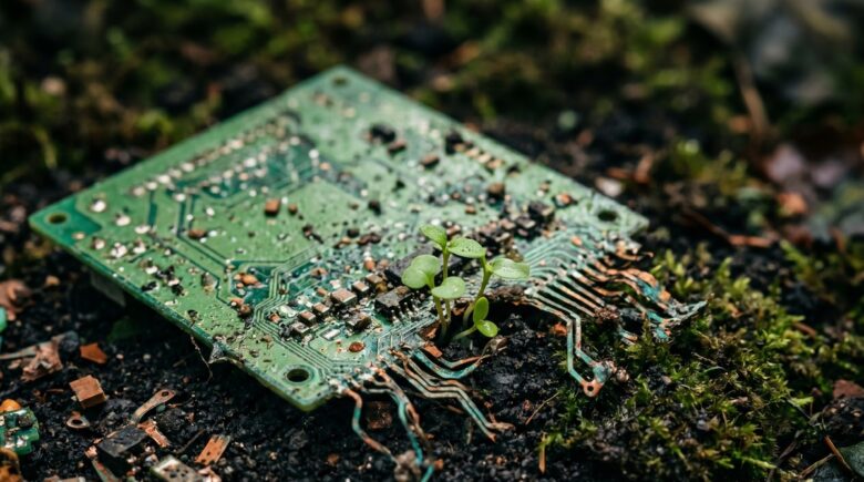
Biodegradable electronics e-waste solutions use plant-based polymers, cellulose, and organic semiconductors to create devices that decompose safely after use. As of July 2025, the global e-waste crisis generates over 62 million metric tons annually, with less than 22.3% formally recycled. Biodegradable electronics directly address this gap by eliminating persistent toxic materials from landfills and waterways.
Biodegradable electronics e-waste is a fast-moving field where engineers design circuit boards, sensors, and wearable devices from materials that break down naturally — reducing the toxic burden of discarded tech. According to the UN Environment Programme’s Global E-Waste Monitor 2024, the world produced 62 million metric tons of electronic waste in 2023, a figure projected to reach 82 million metric tons by 2030. That growth makes scalable, material-level solutions more urgent than ever.
This guide explains exactly how biodegradable electronics work, which materials are leading the charge, where the technology stands commercially, and what challenges remain before it can meaningfully replace conventional devices at scale.
Key Takeaways
- Global e-waste reached 62 million metric tons in 2023, but only 22.3% was formally collected and recycled, according to the UN’s Global E-Waste Monitor 2024.
- Researchers at Stanford University demonstrated a fully biodegradable thin-film transistor made from cellulose nanofibers that degraded in under three weeks in compost conditions, per Nature Electronics.
- The biodegradable electronics market was valued at approximately $847 million in 2023 and is forecast to grow at a CAGR of 9.4% through 2032, according to Precedence Research.
- Electronic waste contains toxic substances including lead, mercury, and cadmium; the U.S. Environmental Protection Agency identifies e-waste as the fastest-growing solid waste stream in the United States.
- Transient electronics — a subset of biodegradable tech — can dissolve in water in as little as 30 minutes, a capability first demonstrated by John Rogers at the University of Illinois and published in Science.
In This Guide
- What Are Biodegradable Electronics and How Do They Work?
- What Materials Make Electronics Biodegradable?
- How Bad Is the E-Waste Problem Biodegradable Electronics Must Solve?
- What Real-World Applications Exist for Biodegradable Electronics?
- What Are the Key Challenges Limiting Biodegradable Electronics?
- What Does the Future of Biodegradable Electronics E-Waste Solutions Look Like?
What Are Biodegradable Electronics and How Do They Work?
Biodegradable electronics are devices engineered from organic or bio-derived materials that decompose — through microbial action, hydrolysis, or enzymatic processes — into non-toxic byproducts after their useful life ends. Unlike conventional electronics, which persist in landfills for centuries, these devices are designed with a programmed end-of-life built into their material composition.
The engineering challenge is significant: electronic components must be stable enough to function reliably during use but unstable enough to degrade predictably afterward. Researchers solve this through transient electronics design, where the substrate, encapsulation layer, or both are made from degradable materials that protect the device during its intended service life.
Transient vs. Partially Biodegradable Devices
Fully transient devices dissolve entirely — substrate, conductors, and semiconductors — once triggered by water, heat, or UV light. Partially biodegradable devices replace only the non-functional structural materials (housings, printed circuit board substrates) with bio-based alternatives while retaining conventional metal interconnects.
Both approaches reduce the biodegradable electronics e-waste footprint, but transient electronics offer the more complete environmental solution. DARPA’s VAPR program (Vanishing Programmable Resources) invested heavily in fully transient military sensors precisely because of this capability.
The concept of transient electronics was pioneered in 2012 by materials scientist John Rogers at the University of Illinois. His team built a silicon-based device on a silk substrate that dissolved completely in saline solution — opening the door to implantable medical electronics that eliminate surgical removal.
What Materials Make Electronics Biodegradable?
The core materials driving biodegradable electronics are plant-derived cellulose, silk fibroin, polylactic acid (PLA), and organic semiconductors derived from carbon-based molecules. Each material offers a different combination of mechanical strength, electrical performance, and degradation timeline.
Substrate Materials
Cellulose nanofibers are among the most promising substrate materials. They are abundant, renewable, and thermally stable up to approximately 200°C — making them compatible with standard semiconductor fabrication processes. Researchers at the University of Wisconsin-Madison demonstrated cellulose nanopaper circuit boards that retain less than 1% of their original volume after composting.
Silk fibroin, derived from silkworm cocoons, is favored for biomedical implants because it degrades in the body at a tunable rate. Its optical clarity and mechanical flexibility also make it useful for flexible display substrates.
Conductive and Semiconducting Materials
Organic semiconductors — including pentacene, rubrene, and PEDOT:PSS — conduct electricity while remaining carbon-based and potentially biodegradable. PEDOT:PSS (poly(3,4-ethylenedioxythiophene) polystyrene sulfonate) is already commercially deposited in printed electronics and has shown biodegradability under industrial composting conditions.
Metallic conductors remain the hardest component to replace. Some research teams are using magnesium and zinc as biodegradable conductor alternatives — both are naturally occurring elements that dissolve harmlessly in biological environments, as documented in Nature Electronics research on transient metal conductors.
| Material | Application | Degradation Time | Key Advantage |
|---|---|---|---|
| Cellulose Nanofiber | PCB substrate | 2–4 weeks (compost) | High thermal stability, abundant |
| Silk Fibroin | Implantable sensors | Days to months (aqueous) | Tunable degradation rate |
| Polylactic Acid (PLA) | Device housing | 3–6 months (industrial compost) | Commercially available at scale |
| Magnesium | Biodegradable conductors | Days to weeks (aqueous) | Non-toxic dissolution products |
| PEDOT:PSS | Organic semiconductor | Months (industrial compost) | High conductivity, printable |
How Bad Is the E-Waste Problem Biodegradable Electronics Must Solve?
The e-waste crisis is the fastest-growing solid waste problem globally, and the scale makes biodegradable electronics e-waste solutions genuinely critical rather than merely aspirational. The EPA classifies e-waste as containing hazardous materials including lead, cadmium, mercury, and brominated flame retardants — all of which leach into soil and groundwater when devices end up in landfills.
Of the 62 million metric tons generated in 2023, only about 13.8 million metric tons were formally processed. The remaining 48 million metric tons were either informally recycled in unsafe conditions, incinerated, or dumped. Low- and middle-income countries bear a disproportionate share of this burden.
The Hidden Cost of Conventional Electronics
A single smartphone contains over 60 chemical elements, many of which are hazardous. The Basel Action Network, a nonprofit watchdog, has documented widespread illegal export of e-waste from high-income nations to West Africa and Southeast Asia, where informal recycling exposes workers to toxic substances.
Wearable technology is a rapidly growing contributor to this waste stream. As explored in our coverage of how wearable technology is transforming personal health tracking, device replacement cycles for wearables can be as short as 18 months — generating significant small-device waste that is almost never formally recycled due to size and complexity.
E-waste is growing at nearly 3 times the rate of any other waste category. At current trajectories, annual global e-waste will exceed 82 million metric tons by 2030, according to the UN’s Global E-Waste Monitor 2024 — making material-level solutions like biodegradable electronics essential, not optional.
What Real-World Applications Exist for Biodegradable Electronics?
Biodegradable electronics e-waste reduction is already happening in four primary application areas: medical implants, environmental sensors, agricultural monitoring, and consumer packaging electronics. Each area has a distinct driver for choosing biodegradable over conventional materials.
Medical Implantable Devices
This is the most commercially advanced category. Biodegradable pressure sensors, temperature monitors, and drug delivery controllers can be implanted, perform their function for a defined period, then dissolve — eliminating the need for a second surgery to remove them. Northwestern University and Washington University in St. Louis have both published clinical research on fully absorbable neural implants.
The FDA has engaged with several manufacturers seeking regulatory pathways for transient implantable devices. The FDA’s Digital Health Center of Excellence provides a framework that increasingly covers bioresorbable device categories.
Environmental and Agricultural Sensors
Biodegradable soil sensors can be distributed across agricultural fields to monitor moisture, pH, and nutrient levels, then left in place to decompose after the growing season. This eliminates the collection logistics that make conventional sensor networks impractical at large scale.
ETH Zurich researchers demonstrated a fully biodegradable humidity and temperature sensor built on a cellulose substrate in 2022, achieving performance comparable to conventional MEMS sensors while degrading completely within 60 days in soil. This kind of precision agriculture application aligns naturally with the broader shift toward sustainable tech infrastructure — much like the edge computing networks discussed in our explainer on what edge computing is and how it works.
“The next generation of electronics will not be defined by performance alone — it will be defined by what happens to the device at end of life. Biodegradable substrates give us a new design dimension that fundamentally changes our relationship with hardware.”
Consumer Packaging and Single-Use Electronics
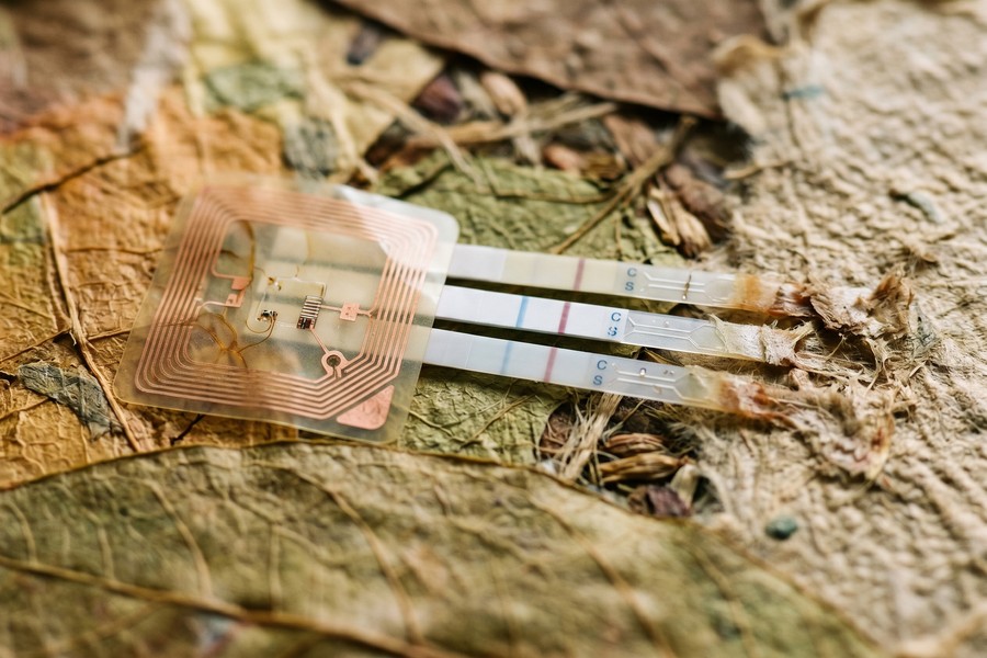
RFID tags, smart labels, and single-use diagnostic strips represent a high-volume, short-lifespan category where biodegradable electronics offer immediate impact. Stora Enso, the Finnish paper and packaging company, has commercialized printed biodegradable RFID antennas on wood-fiber substrates for supply chain tracking. These products already reduce the biodegradable electronics e-waste impact of billions of annual label shipments.
What Are the Key Challenges Limiting Biodegradable Electronics?
Three core challenges currently limit the adoption of biodegradable electronics: performance gaps versus conventional materials, manufacturing scalability, and the difficulty of replacing metal conductors with biodegradable alternatives. These are engineering problems, not fundamental barriers, but they will take years to fully resolve.
Performance and Reliability Gaps
Organic semiconductors typically exhibit carrier mobilities 10 to 100 times lower than silicon. This limits biodegradable electronics to low-frequency, low-power applications for now — sensors, displays, and simple logic circuits rather than high-performance processors. As Nature Electronics has documented, closing this performance gap requires advances in molecular design that remain active research frontiers.
Moisture sensitivity is another constraint. Many biodegradable substrates — by definition — begin to degrade in humid environments. Engineers must balance degradability with adequate shelf life and operational stability, often using thin encapsulation layers that themselves need to be biodegradable.
Manufacturing and Cost Scalability
Conventional semiconductor fabrication is optimized for silicon. Retooling for cellulose or organic semiconductor deposition requires new processes. Roll-to-roll printing has emerged as the leading candidate for scalable biodegradable electronics manufacturing, but yield rates and resolution still lag behind photolithography-based silicon production.
Cost remains a barrier for consumer applications. Biodegradable RFID tags from companies like Stora Enso are cost-competitive for high-volume supply chain use, but more complex biodegradable circuits carry a premium of 2 to 5 times the cost of conventional equivalents at current production volumes.
When evaluating biodegradable electronics products, look specifically for third-party certification of degradation conditions. “Biodegradable” without qualification can mean the device requires industrial composting at 60°C — a condition unavailable in most municipal waste streams. Ask manufacturers for ISO 14855 or ASTM D6400 compliance documentation.
What Does the Future of Biodegradable Electronics E-Waste Solutions Look Like?
The trajectory for biodegradable electronics e-waste solutions points toward mainstream adoption within specific verticals by 2030, with broader consumer electronics applications arriving in the following decade. Three developments will drive this transition: regulatory pressure, material science breakthroughs, and supply chain integration.
Regulatory Drivers
The European Union’s Ecodesign for Sustainable Products Regulation (ESPR), adopted in 2024, creates binding requirements for electronics repairability and recyclability — creating regulatory demand for biodegradable approaches in device design. The European Environment Agency has specifically identified biodegradable substrates as a priority material category under the EU Circular Economy Action Plan.
In the United States, several states have passed extended producer responsibility (EPR) laws for electronics that increase manufacturer incentives to design for end-of-life. As technology grows more deeply integrated into daily life — from the quantum systems covered in our explainer on how quantum computing will change everyday technology to the edge hardware explored in our 5G vs Wi-Fi 7 comparison — the material footprint of connected devices becomes a policy concern that will accelerate biodegradable adoption.
Material Science on the Horizon
Researchers at MIT and IMEC (the Belgian nanoelectronics research center) are actively developing biodegradable gate dielectrics and high-mobility organic semiconductors that could close the performance gap with silicon within five years. Landmark work published in Science has already demonstrated that silicon itself, when fabricated at nanoscale thicknesses, can be made transient — suggesting that the long-term solution may involve thinning silicon rather than replacing it entirely.
The integration of AI-driven materials discovery platforms — where machine learning models predict which molecular structures will yield the optimal combination of electrical performance and degradability — is accelerating development timelines significantly. This mirrors the way AI is reshaping other technology fields, as analyzed in our piece on how AI is changing internet search.
Frequently Asked Questions
Are biodegradable electronics currently available to buy?
Yes, in limited commercial categories. Biodegradable RFID tags, smart packaging labels, and some medical sensors are commercially available from companies including Stora Enso and several biomedical device manufacturers. Consumer electronics with fully biodegradable components remain in advanced research and prototype stages as of mid-2025.
How long do biodegradable electronics take to decompose?
Degradation time varies by material and environment. Silk fibroin devices can dissolve in aqueous conditions in days to weeks. Cellulose-based substrates typically degrade in two to four weeks under industrial composting conditions. PLA housings require three to six months at elevated temperatures in certified industrial composting facilities — they do not break down quickly in home compost or landfills.
Do biodegradable electronics perform as well as conventional ones?
Not yet for high-performance applications. Current biodegradable electronics are best suited for low-power, low-frequency applications such as sensors, displays, and RFID. Organic semiconductors have carrier mobilities significantly lower than silicon. However, for many IoT and medical sensing applications, this performance level is entirely sufficient.
What happens to the metals inside biodegradable electronics?
This is the central unsolved challenge. Researchers are replacing copper and gold with magnesium, zinc, and iron — metals that dissolve harmlessly in biological environments. However, many current biodegradable electronics still use small amounts of conventional metals for high-performance interconnects, meaning they are only partially biodegradable until this substitution is complete.
What is the difference between biodegradable and recyclable electronics?
Recyclable electronics are designed to have materials recovered and reused in new products — this requires formal collection and processing infrastructure that currently handles less than 22.3% of global e-waste. Biodegradable electronics decompose naturally without requiring infrastructure, making them a complementary rather than competing approach to the e-waste problem.
Are biodegradable electronics safe to dispose of in regular compost?
Most require industrial composting conditions — typically temperatures above 55°C — rather than home composting. Devices certified to ASTM D6400 or EN 13432 standards meet industrial compostability benchmarks. Always check manufacturer specifications. Disposing of electronics that contain even small metal components in home compost is not recommended until conductor substitution is fully resolved.
Which companies are leading biodegradable electronics development?
Stora Enso leads in biodegradable RFID and printed electronics for packaging. In biomedical devices, Roper Technologies and several university spinouts are active. Research leadership is concentrated at Stanford, MIT, Northwestern, ETH Zurich, and IMEC. No single company currently dominates the full spectrum of biodegradable electronics categories.
Sources
- UN Environment Programme — Global E-Waste Monitor 2024
- Nature Electronics — Biodegradable and Transient Electronic Devices
- Science — A Physically Transient Form of Silicon Electronics (Rogers et al.)
- U.S. Environmental Protection Agency — Cleaning Up Electronic Waste (E-Waste)
- Precedence Research — Biodegradable Electronics Market Size and Forecast
- U.S. FDA — Digital Health Center of Excellence: What Is Digital Health
- European Environment Agency — Waste Topics and Circular Economy Data
- Basel Convention — E-Waste Overview and International Controls