Fact-checked by the VisualEnews editorial team
Quick Answer
Photonic chips technology uses light instead of electrons to transmit and process data, delivering speeds up to 100 times faster than conventional silicon chips while consuming up to 90% less energy. As of July 2025, companies like Intel, IBM, and Lightmatter are deploying commercial photonic processors that are reshaping AI infrastructure and data center performance.
Photonic chips technology represents the most significant shift in processor architecture since the transistor. Rather than moving electrons through copper wires, photonic chips route photons — particles of light — through silicon waveguides, eliminating the resistance and heat that throttle traditional chips. According to a 2022 benchmark study published in Nature Photonics, photonic interconnects have demonstrated data transfer rates exceeding 1 terabit per second in laboratory conditions.
The timing matters. As AI model sizes double roughly every six months and data center electricity costs surge, photonic processing offers a rare combination of higher throughput and lower thermal output — two problems that silicon has struggled to solve simultaneously.
How Do Photonic Chips Actually Work?
Photonic chips encode data as pulses of light rather than electrical voltage, then process that data using optical components — waveguides, modulators, and photodetectors — etched onto a silicon substrate. The core principle is that photons travel at the speed of light and do not collide with each other, eliminating the cross-talk and resistance that degrade electronic signals.
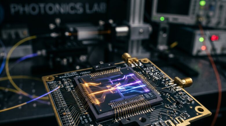
Key Components Inside a Photonic Processor
A silicon photonic chip typically contains three functional layers. The modulator layer converts electrical input signals into optical pulses. The waveguide network routes those pulses across the chip. Finally, the photodetector layer converts light back into electrical signals for output. This hybrid architecture — often called co-packaged optics — allows photonic chips to interface with existing electronic infrastructure without requiring a full system redesign.
Intel’s Integrated Photonics Solutions Group has been co-packaging optical transceivers directly onto processor dies since 2023, reducing signal latency between compute and memory by an estimated 40% according to Intel’s integrated photonics research documentation.
Key Takeaway: Photonic chips process data as light pulses through silicon waveguides, not electrical signals. Intel’s co-packaged optics approach has demonstrated 40% lower latency between compute and memory, according to Intel’s photonics research, making this architecture immediately viable for data centers.
How Fast Are Photonic Chips Compared to Silicon?
Photonic chips can move data at speeds that current electronic chips simply cannot match at equivalent power budgets. In practical deployments, photonic interconnects operate at 800 Gbps to 1.6 Tbps per fiber, while standard copper interconnects max out near 112 Gbps before signal degradation becomes unmanageable.
The gap widens at scale. When hundreds of GPU or TPU nodes need to communicate in an AI training cluster, electronic interconnects become the bottleneck — not the processors themselves. Photonic chips technology dissolves that bottleneck. Lightmatter, a Boston-based photonics startup valued at over $4.4 billion after its 2024 funding round, has built an optical interconnect fabric called Passage that links AI chips with photonic bandwidth, demonstrating a 10x improvement in tokens processed per watt in large language model inference tasks.
| Technology | Max Bandwidth | Power per Gbps | Latency |
|---|---|---|---|
| Photonic Interconnect | 1,600 Gbps | 0.5 pJ/bit | Sub-nanosecond |
| Copper Electrical | 112 Gbps | 5–10 pJ/bit | 2–5 nanoseconds |
| Standard Fiber (External) | 400 Gbps | 1.2 pJ/bit | 1–3 nanoseconds |
| NVIDIA NVLink (Electrical) | 900 Gbps | 3–4 pJ/bit | 1–2 nanoseconds |
“Photonic interconnects are not a distant future — they are the present solution to the bandwidth wall. Every major hyperscaler is already piloting co-packaged optics because the math on power and speed is simply undeniable.”
Key Takeaway: Photonic interconnects deliver up to 1,600 Gbps of bandwidth at roughly one-tenth the energy per bit of copper alternatives. Lightmatter’s Passage fabric achieved a 10x improvement in AI inference efficiency, signaling that commercial photonic deployment is already underway.
Who Is Leading Photonic Chips Technology?
A concentrated group of semiconductor giants and well-funded startups currently dominates the photonic chips technology landscape. Intel, IBM, and TSMC are leading on the manufacturing side, while Lightmatter, Ayar Labs, and PsiQuantum are advancing the application layer.
Major Players and Their Approaches
IBM has integrated photonic components into its quantum computing roadmap, using optical interconnects to link cryogenic QPUs to room-temperature control electronics. TSMC offers a silicon photonics process node — known as SiPho — that allows fabless chip designers to tape out photonic designs on the same production lines used for advanced CMOS logic. This dramatically lowers the barrier to entry for startups.
Ayar Labs, backed by NVIDIA and Intel Capital, has developed an in-package optical I/O chiplet that plugs into standard processor sockets. Their TeraPHY chiplet delivers 2 Tbps of optical bandwidth in a package small enough to sit beside a GPU die. This kind of modularity is critical: it means photonic chips technology can enhance existing hardware rather than replace it outright. For a broader view of how next-generation computing architectures are evolving, see our overview of how quantum computing will change everyday technology.
Key Takeaway: TSMC’s SiPho process node and Ayar Labs’ TeraPHY chiplet — delivering 2 Tbps of optical bandwidth — are making photonic chips technology manufacturable at scale without exotic fabrication, according to Ayar Labs’ TeraPHY product documentation.
What Are the Current Limits of Photonic Chips?
Photonic chips technology still faces three stubborn engineering challenges: optical loss, thermal sensitivity, and the difficulty of performing nonlinear computation in the optical domain. These are real constraints — not reasons to dismiss the technology, but factors that define where it excels and where it still lags.
Optical loss occurs when photons scatter inside waveguides, degrading signal strength over distance. State-of-the-art silicon waveguides still exhibit propagation losses of roughly 1–3 dB per centimeter, which limits chip size. Thermal drift is another issue: silicon’s refractive index changes with temperature, which shifts the wavelength of optical signals and causes errors. Active thermal stabilization adds power overhead that partially erodes the energy efficiency advantage.
The Computation Bottleneck
Perhaps the deepest limitation is that light does not naturally perform the nonlinear operations — like activation functions in neural networks — that digital computation requires. Most photonic chips today handle data movement and matrix multiplication in the optical domain, then hand off to electronic circuits for nonlinear steps. This hybrid model adds latency and complexity. Research groups at Stanford University and MIT are exploring materials like lithium niobate and indium phosphide that could enable all-optical nonlinear computation, but commercial readiness remains 3–5 years away by most analyst estimates.
Understanding these tradeoffs is similar to evaluating other hardware decisions — just as buyers weigh speed versus longevity when choosing between solid state drives and hard drives, engineers must weigh photonic throughput against integration complexity.
Key Takeaway: Silicon photonic waveguides still lose 1–3 dB per centimeter of signal, and full all-optical computation is 3–5 years from commercial viability. Today’s photonic chips are most effective as interconnect accelerators, not standalone replacements for conventional electronic integrated circuits.
How Will Photonic Chips Impact AI and Data Centers?
Photonic chips technology is poised to reshape AI infrastructure more than any other single hardware innovation in the near term. The bottleneck in large-scale AI training and inference is no longer the GPU — it is moving data between GPUs fast enough to keep them all busy. Photonics solves exactly that problem.
The U.S. Department of Energy’s data center energy consumption reports project that AI workloads will push U.S. data center electricity use to over 200 terawatt-hours per year by 2026. Photonic interconnects, by cutting per-bit energy by up to 90%, could prevent a significant share of that demand growth. Hyperscalers including Google, Microsoft, and Amazon Web Services are all actively investing in co-packaged optics programs, according to industry reporting from Light Reading’s telecom and photonics desk.
The ripple effects extend beyond data centers. Edge computing deployments — where latency and power are tightly constrained — stand to benefit enormously. For more on how distributed processing architectures are evolving, see our explainer on what edge computing is and how it works. Similarly, the wireless infrastructure underpinning 5G networks will require photonic backhaul to meet throughput demands — a connection explored in our breakdown of 5G versus Wi-Fi 7.
Key Takeaway: U.S. data centers are on track to consume over 200 TWh of electricity annually by 2026. Photonic chips technology cuts per-bit energy by up to 90%, making it the most credible near-term solution to AI’s power crisis, per U.S. Department of Energy projections.
Frequently Asked Questions
What are photonic chips and how do they differ from regular chips?
Photonic chips use light — photons — instead of electrical signals to transmit and process data. Unlike conventional silicon chips that move electrons through copper wires, photonic chips route light through waveguides, achieving far higher speeds and lower energy consumption. The core advantage is that photons travel without resistance and can carry multiple data streams simultaneously on different wavelengths.
Are photonic chips available commercially right now?
Yes, in specific applications. As of 2025, Intel, Ayar Labs, and Lightmatter offer commercially available photonic components targeting data center interconnects and AI accelerator clusters. Full all-optical processors that handle both data movement and computation are still in advanced research phases, with commercial readiness projected between 2027 and 2030.
Can photonic chips replace CPUs and GPUs?
Not yet — and possibly never entirely. Today’s photonic chips excel at data movement and matrix multiplication, which makes them powerful accelerators for AI inference. However, the nonlinear operations required for general-purpose computing are still handled by electronic circuits. The near-future architecture is hybrid: photonic interconnects paired with electronic processors.
How much faster is a photonic chip than a traditional processor?
For data transfer, photonic interconnects operate at 800 Gbps to 1.6 Tbps per channel, compared to roughly 112 Gbps for state-of-the-art copper electrical links. For AI matrix operations, photonic chips have demonstrated up to 100x greater throughput per watt in controlled benchmarks, though real-world gains depend heavily on workload type.
Which companies are investing most heavily in photonic chips technology?
Intel, IBM, and TSMC lead on the manufacturing side. On the startup side, Lightmatter (valued at $4.4 billion), Ayar Labs (backed by NVIDIA and Intel Capital), and PsiQuantum (focused on photonic quantum computing) are the most capitalized players. Google, Microsoft, and Amazon Web Services are all running internal co-packaged optics programs as well.
What is the biggest technical barrier to photonic chips scaling up?
The primary barrier is the inability of current photonic materials to perform nonlinear optical computation efficiently. Silicon’s refractive index also shifts with temperature, causing signal errors that require active correction. Researchers at MIT and Stanford are exploring lithium niobate and indium phosphide substrates as potential solutions, with commercial results expected within 3 to 5 years.
Sources
- Nature Photonics — Silicon Photonic Interconnect Benchmarks (2022)
- Intel — Integrated Photonics Research Overview
- Ayar Labs — TeraPHY In-Package Optical I/O Product Page
- U.S. Department of Energy — Data Centers and Servers Energy Projections
- Lightmatter — Passage Optical Interconnect Fabric
- Light Reading — Photonics and Telecom Infrastructure Reporting
- Wikipedia — Silicon Photonics: Technology Overview