Fact-checked by the VisualEnews editorial team
Quick Answer
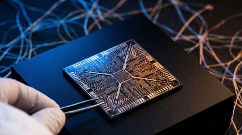
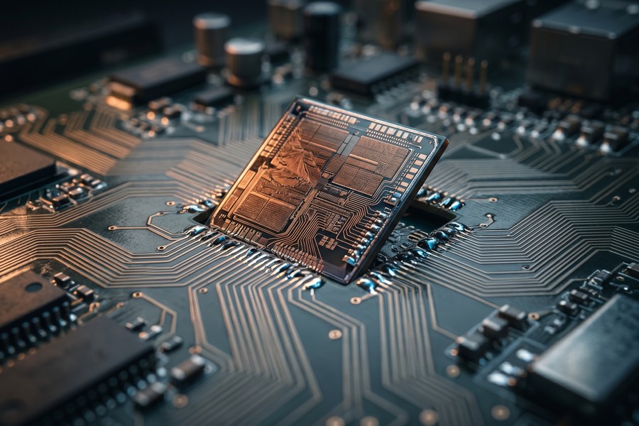
Neuromorphic chips explained in brief: these are brain-inspired processors that mimic the structure of biological neurons to perform computing tasks using a fraction of the energy of traditional chips. As of July 2025, neuromorphic processors like Intel’s Loihi 2 can be 1,000x more energy-efficient than conventional CPUs for specific AI workloads, processing data in real time with as few as 1 milliwatt of power.
Neuromorphic chips explained simply: they are specialized semiconductors designed to replicate how the human brain processes information — using interconnected artificial neurons and synapses instead of the transistor-based logic gates found in traditional processors. As of July 2025, the neuromorphic computing market is valued at approximately $68 million and projected to exceed $630 million by 2030, according to MarketsandMarkets research. This technology sits at the intersection of neuroscience, computer engineering, and artificial intelligence — and it is quietly reshaping how machines learn.
Why does this matter right now? The AI hardware race is intensifying. As large language models and edge AI applications demand lower power consumption, traditional GPU-based systems are hitting a wall. Neuromorphic chips offer a path forward — processing sparse, event-driven data in ways that consume dramatically less energy than today’s power-hungry data centers. Companies like Intel, IBM, BrainChip Holdings, and research groups at institutions like MIT and Stanford University are racing to commercialize the technology.
This guide is written for technology enthusiasts, students, and curious professionals who want a clear, jargon-free foundation in neuromorphic computing. By the end, you will understand how these chips work, why they matter, how they compare to conventional and quantum processors, and where they are already being deployed in the real world.
Key Takeaways
- Neuromorphic chips use spiking neural networks (SNNs) to process information, consuming as little as 1 milliwatt of power — compared to hundreds of watts for a typical GPU, according to Intel’s neuromorphic research division.
- Intel’s Loihi 2 chip contains 1 million artificial neurons and 120 million synaptic connections, making it one of the most advanced neuromorphic processors available as of 2025, per Intel Research.
- IBM’s NorthPole chip, announced in 2023, achieved 22x better energy efficiency per unit of performance than leading GPU architectures on inference tasks, according to a study published in Science Magazine.
- The neuromorphic computing market is forecast to grow at a CAGR of 55.9% between 2025 and 2030, driven by demand for low-power edge AI, per MarketsandMarkets 2024.
- BrainChip’s Akida processor processes vision, audio, and sensor data at the edge using under 30 milliwatts, enabling always-on AI in battery-powered devices without cloud connectivity, per BrainChip’s technical documentation.
- Neuromorphic systems are already deployed in real-world applications including prosthetic limb control, autonomous vehicle sensor fusion, and industrial anomaly detection, according to research compiled by the Defense Advanced Research Projects Agency (DARPA).
In This Guide
- Step 1: What Are Neuromorphic Chips and How Do They Actually Work?
- Step 2: How Are Neuromorphic Chips Different From Regular CPUs and GPUs?
- Step 3: What Are Neuromorphic Chips Actually Being Used For Right Now?
- Step 4: Which Companies and Research Labs Are Leading Neuromorphic Chip Development?
- Step 5: How Do Neuromorphic Chips Compare to Quantum Computing?
- Step 6: What Are the Biggest Limitations of Neuromorphic Chips Today?
- Step 7: Will Neuromorphic Chips Replace GPUs for AI Workloads in the Future?
- Frequently Asked Questions
Step 1: What Are Neuromorphic Chips and How Do They Actually Work?
Neuromorphic chips are processors designed to replicate the architecture and operating principles of the human brain, using artificial neurons and synapses implemented in silicon. Unlike conventional chips that operate on binary clock cycles, neuromorphic processors communicate via spikes — brief electrical pulses that fire only when needed, mimicking how biological neurons transmit signals.
How to Understand the Core Mechanism
The foundational concept behind neuromorphic computing is the Spiking Neural Network (SNN). In an SNN, artificial neurons accumulate input signals over time. When the accumulated signal crosses a threshold, the neuron “fires” a spike and resets — exactly as a biological neuron does. This event-driven model means the chip only consumes energy when activity occurs, rather than continuously cycling through clock ticks.
The term “neuromorphic” was coined by physicist Carver Mead of the California Institute of Technology in the late 1980s. Mead demonstrated that analog circuits could model biological neural computation far more efficiently than digital logic. His foundational work laid the groundwork for every commercial neuromorphic chip built today.
Each artificial neuron on a neuromorphic chip connects to thousands of others via programmable synapses — weighted connections that strengthen or weaken based on usage, a property known as synaptic plasticity. This allows the chip to learn from experience directly in hardware, without requiring a separate training phase on a GPU cluster.
What to Watch Out For
A common misconception is that neuromorphic chips are simply “brain simulations.” They are not. They are physical hardware architectures inspired by neural principles — not digital models of the brain. The distinction matters because it affects how they are programmed and what tasks they excel at versus struggle with.
The human brain contains approximately 86 billion neurons and 100 trillion synaptic connections, yet operates on only about 20 watts of power — roughly the same as a dim light bulb. Neuromorphic chips aim to approach this extraordinary efficiency ratio in silicon.
Step 2: How Are Neuromorphic Chips Different From Regular CPUs and GPUs?
Neuromorphic chips differ fundamentally from CPUs and GPUs in architecture, communication model, and energy behavior. Where CPUs execute sequential instructions and GPUs parallelize matrix math, neuromorphic chips process sparse, asynchronous events — making them uniquely suited for real-time sensory data, not bulk number crunching.
How to Think About the Architectural Difference
A CPU (Central Processing Unit) follows the von Neumann architecture: it fetches data from memory, processes it in a core, and writes results back. This memory-processor bottleneck, known as the “von Neumann bottleneck,” causes significant energy waste. A GPU (Graphics Processing Unit) improves parallelism by running thousands of cores simultaneously — ideal for training deep learning models but extremely power-hungry, with flagship models like the NVIDIA H100 consuming up to 700 watts.
Neuromorphic chips dissolve the memory-processor divide entirely. Memory and computation are co-located at each neuron node, eliminating the bottleneck. This architecture, sometimes called in-memory computing, slashes energy use dramatically for tasks involving continuous sensory streams.
For readers who want deeper context on how hardware architectures affect everyday tech, our overview of solid state drives vs hard drives explores how storage architecture similarly dictates performance trade-offs.
What to Watch Out For
Neuromorphic chips are not general-purpose replacements for CPUs or GPUs. They underperform on tasks requiring dense matrix multiplication — like training large language models. Their advantage is narrow but powerful: real-time inference on sparse, time-varying data with minimal energy.
IBM’s NorthPole neuromorphic chip delivers 22x better energy efficiency per inference operation than a leading GPU architecture, while eliminating off-chip memory access entirely, according to research published in Science Magazine in 2023.
| Processor Type | Architecture | Typical Power Draw | Best Use Case | AI Training Capable? |
|---|---|---|---|---|
| Neuromorphic Chip (e.g., Loihi 2) | Spiking neural network, in-memory compute | 1–30 mW | Real-time edge inference, sensory AI | Limited (on-chip learning only) |
| CPU (e.g., Intel Core i9) | Von Neumann, sequential | 65–253 W | General-purpose computing, OS tasks | Slow but capable |
| GPU (e.g., NVIDIA H100) | Massively parallel, CUDA cores | 350–700 W | AI model training, graphics rendering | Yes (primary use case) |
| Edge TPU (e.g., Google Coral) | Fixed-function matrix accelerator | 2–4 W | Edge inference for TensorFlow Lite models | No (inference only) |
| Quantum Processor (e.g., IBM Eagle) | Quantum gates, qubit superposition | Requires cryogenic cooling (~15 kW system) | Optimization, cryptography, simulation | Experimental only |
The table above makes clear that no single chip type dominates all use cases. Neuromorphic processors occupy a specific niche — one that is growing rapidly as edge AI and IoT deployment scales.
Step 3: What Are Neuromorphic Chips Actually Being Used For Right Now?
Neuromorphic chips are not purely experimental — they are already deployed in production environments across robotics, healthcare, defense, and consumer electronics. The most commercially active applications involve always-on sensory processing, where low power consumption is non-negotiable.
How to Identify Current Use Cases
Prosthetics and neural interfaces represent one of the most impactful early applications. Researchers at the University of Southern California have used Intel’s Loihi platform to process sensory feedback from prosthetic limbs in real time, allowing amputees to feel texture and pressure. The chip’s spike-based processing matches the natural timing of biological nerve signals far better than traditional DSPs.
Autonomous vehicle sensor fusion is another active deployment zone. BrainChip’s Akida processor is being tested in automotive applications to process data from event cameras — sensors that fire pixel-level updates only when motion is detected. This approach reduces the data pipeline by up to 90% compared to frame-based cameras, lowering both latency and energy load.
In the industrial sector, neuromorphic chips enable predictive maintenance by analyzing vibration, thermal, and acoustic sensor streams continuously at the edge. Because the chip only activates when anomalous patterns appear, factories can run always-on monitoring without draining power budgets. This connects naturally to broader trends in edge computing architectures that push intelligence to the device level.
Smart hearing aids are perhaps the most commercially mature consumer application. Companies like GN Audio have integrated neuromorphic-inspired processing to separate speech from background noise in real time, with power budgets under 1 mW — a requirement that makes conventional DSPs impractical.
What to Watch Out For
Most current neuromorphic deployments are in narrow, well-defined domains. Claims about neuromorphic chips replacing general AI systems are premature. The technology excels at pattern recognition on time-series data — not at language generation or image synthesis tasks that require dense, high-precision arithmetic.
If you are evaluating neuromorphic hardware for a project, focus on workloads characterized by sparse, asynchronous input — like keyword spotting, gesture recognition, or anomaly detection. These are the tasks where neuromorphic chips deliver 10x to 1,000x energy gains over GPU-based alternatives.
Step 4: Which Companies and Research Labs Are Leading Neuromorphic Chip Development?
The neuromorphic chip landscape is dominated by a small number of well-funded players — Intel and IBM on the corporate side, with significant contributions from academic institutions and defense-backed research programs. Understanding who is building what helps clarify where the technology is heading.
How to Map the Ecosystem
Intel’s Neuromorphic Research Community (INRC) is the largest open research program in the field. Intel’s second-generation Loihi 2 chip, fabricated on Intel’s 4nm process, contains 1 million neurons and 120 million synapses. Intel has shipped over 200 Loihi systems to partner research institutions globally, enabling work in robotics, olfaction, and optimization problems.
IBM Research has pursued two distinct neuromorphic trajectories. Its legacy TrueNorth chip, released in 2014, packed 4,096 neurosynaptic cores and 1 million programmable neurons onto a single chip consuming just 70 milliwatts. IBM’s newer NorthPole architecture, detailed in a landmark 2023 paper, pushed the energy efficiency frontier further by co-locating all memory on-chip.
BrainChip Holdings (ASX: BRN) is the only publicly listed pure-play neuromorphic chip company. Its Akida NSoC (Neuromorphic System-on-Chip) targets commercial edge AI markets and has secured design wins in automotive, industrial IoT, and consumer electronics sectors. The chip processes vision and audio using under 30 milliwatts.
On the research front, DARPA’s Microsystems Technology Office has funded multiple neuromorphic programs under initiatives like HIVE (Hierarchical Identify Verify Exploit) and FRANC (Future Architectures for Neuromorphic Computing), with the explicit goal of achieving 1,000x improvements in computational efficiency over conventional architectures.
Stanford University’s Neurogrid project and MIT’s Research Laboratory of Electronics remain key academic contributors, regularly publishing foundational work on analog neuromorphic circuits and on-chip learning algorithms.
“Neuromorphic computing is not just about making AI faster — it is about making intelligence sustainable. The brain processes the world using a billionth of the energy that current AI chips require. That gap is our opportunity.”
What to Watch Out For
Many “neuromorphic” product announcements blend marketing with engineering reality. A chip that uses analog circuits or spike-inspired processing is not necessarily a true neuromorphic device. Look for disclosure of SNN support, on-chip learning capability, and published benchmark results on standardized tasks like those in the Open Neuromorphic benchmark suite.
Investor announcements from smaller neuromorphic startups frequently overstate capabilities. Before drawing conclusions about commercial readiness, verify whether the chip has been independently benchmarked and whether production volumes — not just prototype runs — have been achieved.
Step 5: How Do Neuromorphic Chips Compare to Quantum Computing?
Neuromorphic and quantum computing are frequently lumped together as “next-generation computing,” but they solve entirely different problems using entirely different physics. Understanding the distinction prevents misplaced expectations about what each technology can deliver.
How to Understand the Difference
Quantum computing manipulates quantum bits (qubits) that can exist in superposition — representing 0, 1, or both simultaneously. This enables exponential speedups on specific problem classes: integer factorization, quantum chemistry simulation, and certain optimization tasks. However, quantum processors currently require cooling to near absolute zero (-273.14°C), making them datacenter-bound research tools. For a deeper introduction to where quantum hardware is headed, see our guide on how quantum computing will change everyday technology.
Neuromorphic computing, by contrast, operates at room temperature, consumes milliwatts of power, and is designed to run continuously at the edge of networks — inside smartphones, drones, medical implants, and industrial sensors. Its advantage is not raw computational power but energy-efficient, real-time inference on sensory streams.
The two technologies are complementary, not competitive. A future AI system might use quantum processors for complex optimization during training, neuromorphic chips for always-on edge inference, and classical GPUs for bulk matrix operations — each layer handling what it does best.
What to Watch Out For
Media coverage routinely conflates “post-silicon computing” technologies. Quantum computing will not replace neuromorphic chips, and vice versa. They occupy different positions in the computing stack and serve different workloads entirely.
While quantum computers require elaborate cryogenic systems consuming tens of kilowatts just to maintain operating temperature, a neuromorphic chip like Intel’s Loihi 2 fits on a circuit board the size of a USB drive and runs on a standard 5-volt power supply — with milliwatt-level inference power draw.
Step 6: What Are the Biggest Limitations of Neuromorphic Chips Today?
Neuromorphic chips face real, substantial barriers to mainstream adoption — from software ecosystem immaturity to programming complexity. Acknowledging these limitations honestly is essential for anyone evaluating the technology seriously.
How to Assess the Barriers
The most significant challenge is the software and toolchain gap. Conventional AI development relies on mature frameworks like TensorFlow, PyTorch, and ONNX — none of which natively support spiking neural networks. Intel offers its own Lava software framework for Loihi, and BrainChip provides the MetaTF toolkit, but both require steep learning curves and lack the community size of mainstream AI tools.
A second barrier is programmability. Training SNNs effectively remains an open research problem. Standard backpropagation — the dominant training algorithm for deep learning — does not translate directly to spike-based networks because spikes are discrete events, not differentiable functions. Researchers use workarounds like surrogate gradient methods, but these add complexity and reduce training efficiency.
Third, standardization is absent. There is no equivalent of the CUDA programming model — which made NVIDIA GPUs the universal platform for AI research — in the neuromorphic world. Each chip vendor uses proprietary APIs, making code non-portable between Intel, IBM, and BrainChip systems. This fragmentation slows ecosystem growth substantially.
Finally, current neuromorphic chips have limited precision. Spiking networks typically operate with low-bit-width representations, which constrains their performance on tasks requiring high numerical accuracy, such as financial modeling or scientific simulation.
What to Watch Out For
The software gap is the single largest practical barrier for developers today. Before committing to a neuromorphic platform, audit whether the vendor provides actively maintained SDKs, community forums, and pre-trained model libraries. Without these, development timelines extend dramatically.
“The hardware has outpaced the software. We have chips capable of remarkable efficiency gains, but the programming models to unlock that potential are still catching up. Closing that gap is the defining challenge of the next five years in neuromorphic engineering.”
Step 7: Will Neuromorphic Chips Replace GPUs for AI Workloads in the Future?
Neuromorphic chips are unlikely to replace GPUs for general AI workloads, but they will capture a large and growing share of edge AI deployment — particularly where energy, latency, and always-on operation are the binding constraints. The realistic future is a heterogeneous computing stack, not a single winner.
How to Think About the Trajectory
The immediate growth vector for neuromorphic chips is edge AI — intelligence embedded in devices rather than processed in the cloud. As wearable health technology becomes more sophisticated, devices like continuous glucose monitors, hearing aids, and neural interfaces will require persistent, low-power AI that cloud-dependent GPUs cannot economically provide.
The broader AI infrastructure context also favors neuromorphic growth. As noted in analyses of how AI is transforming internet search, the compute demands of AI deployment are escalating rapidly — and energy costs are becoming a strategic constraint for every major technology company. Neuromorphic chips offer a route to inference at scale without proportional energy cost increases.
Industry analysts at Gartner have positioned neuromorphic computing on their emerging technology hype cycle, projecting that the technology reaches the “Slope of Enlightenment” — meaning meaningful commercial adoption — within 5 to 10 years from 2024. The CAGR of 55.9% forecast through 2030 reflects early but accelerating commercial momentum.
The most likely near-term outcome is neuromorphic chips serving as specialized co-processors alongside CPUs in edge devices — similar to how Neural Processing Units (NPUs) have been integrated into Apple’s M-series chips and Qualcomm’s Snapdragon platforms. The neuromorphic chip may not replace the GPU, but it will sit beside it in the AI hardware hierarchy.
What to Watch Out For
Watch for neuromorphic IP being absorbed into larger semiconductor roadmaps. Intel’s neuromorphic research could influence future Meteor Lake or Nova Lake architectures. Similarly, NVIDIA has filed neuromorphic-adjacent patents suggesting the boundary between GPU and neuromorphic design may blur over time.
If you follow AI hardware trends professionally, track neuromorphic chip developments alongside edge computing and IoT hardware news — not alongside GPU benchmarks. The competitive landscape is different, the customers are different, and the use cases are distinct from datacenter AI acceleration.
Frequently Asked Questions
What are neuromorphic chips explained in the simplest possible terms?
Neuromorphic chips are computer processors built to work like a brain — using artificial neurons that send spike signals to each other, rather than running calculations on a fixed clock cycle. This approach lets the chip process real-world sensory data using far less energy than a conventional processor. Intel’s Loihi 2, for example, runs AI inference workloads using as little as 1 milliwatt, compared to hundreds of watts for a GPU doing equivalent tasks.
Can neuromorphic chips run ChatGPT or large language models?
No — current neuromorphic chips cannot run large language models like ChatGPT or GPT-4. These models require dense, high-precision matrix multiplication across billions of parameters, which neuromorphic architectures are not optimized for. Neuromorphic chips excel at sparse, event-driven pattern recognition tasks — like keyword detection, motion sensing, and anomaly identification — rather than generative text or image synthesis.
How much do neuromorphic chips cost to buy or develop with?
Access to neuromorphic hardware for developers is currently gated through research programs rather than open commercial sales. Intel provides Loihi 2 hardware through its Intel Neuromorphic Research Community at no direct cost to approved academic and corporate partners. BrainChip’s Akida development kits are available commercially, with evaluation board pricing starting around $350 USD as of 2025. Full production volumes for embedded applications require direct vendor engagement and vary by order size.
Are neuromorphic chips the same as AI chips or machine learning accelerators?
Neuromorphic chips are a specific subset of AI hardware, but they are architecturally distinct from conventional AI accelerators like Google’s TPU or NVIDIA’s Tensor Cores. Standard AI accelerators optimize matrix math using fixed-precision arithmetic. Neuromorphic chips use spiking neural networks and event-driven computation — a fundamentally different computational paradigm. The two types of chips are complementary rather than interchangeable.
What programming language do you use to program neuromorphic chips?
Neuromorphic chips are programmed using vendor-specific frameworks rather than standard languages. Intel’s Loihi 2 uses the Lava open-source framework, which is Python-based and available on GitHub via the lava-nc project. BrainChip’s Akida platform uses the MetaTF toolkit, which bridges TensorFlow models to spike-compatible representations. There is currently no universal neuromorphic programming standard equivalent to CUDA for NVIDIA GPUs.
How energy efficient are neuromorphic chips compared to traditional AI hardware?
Neuromorphic chips are dramatically more energy efficient for inference on sparse, real-time data — consuming between 1 and 30 milliwatts for tasks that require 30 to 700 watts on GPU hardware. IBM’s NorthPole demonstrated 22x better energy efficiency per inference operation compared to a leading GPU architecture in benchmarks published in Science Magazine in 2023. The efficiency gap narrows significantly on dense, compute-heavy workloads like large model training, where neuromorphic chips currently cannot compete.
Is neuromorphic computing related to quantum computing?
Neuromorphic and quantum computing are two separate, unrelated hardware paradigms that are both classified as “next-generation computing.” Neuromorphic chips are classical silicon hardware running at room temperature, designed for energy-efficient sensory AI. Quantum computers manipulate qubits using quantum mechanical properties and require cooling to near absolute zero. They solve different problem types and are not competing technologies — they are likely to be used together in future hybrid computing systems.
Which industries will benefit most from neuromorphic chips in the next five years?
The industries positioned to benefit most from neuromorphic chips between 2025 and 2030 are healthcare (neural prosthetics, always-on health monitoring), automotive (event-camera sensor fusion for autonomous vehicles), industrial IoT (predictive maintenance on edge sensors), and defense (low-power battlefield AI). The neuromorphic market is forecast to grow at a CAGR of 55.9% through 2030, with edge AI and IoT applications driving the majority of commercial revenue, according to MarketsandMarkets 2024 analysis.
Can neuromorphic chips learn on the device without cloud connectivity?
Yes — on-chip learning is one of the defining capabilities of neuromorphic chips, and it is a key advantage over conventional AI hardware. Intel’s Loihi 2 supports several on-chip learning algorithms, including spike-timing-dependent plasticity (STDP), which allows the chip to update synaptic weights in real time based on incoming data. This enables neuromorphic chips to adapt to new patterns locally — without sending data to a cloud server — which is critical for privacy-sensitive applications like medical devices and personal wearables. For context on how edge-level intelligence fits broader technology trends, see our overview of edge computing and how it works.
Sources
- Intel Research — Neuromorphic Computing and Loihi 2
- Science Magazine — IBM NorthPole: Neural Inference at the Frontier of Energy and Spatial Efficiency (2023)
- MarketsandMarkets — Neuromorphic Computing Market Global Forecast to 2030
- BrainChip Holdings — Akida Neuromorphic System-on-Chip Technology
- DARPA — Systems-Based Neurotechnology for Emerging Therapies (SUBNETS)
- NVIDIA — H100 Tensor Core GPU Architecture and Specifications
- Intel Lava Framework — Open-Source Neuromorphic Computing Software (GitHub)
- Wikipedia — Neuromorphic Engineering (Carver Mead and Foundational History)
- IBM Research Blog — NorthPole: A Brain-Inspired Chip for AI
- Gartner — Emerging Technology Hype Cycle Methodology and Neuromorphic Positioning