Fact-checked by the VisualEnews editorial team
Quick Answer
Photonic chips use light instead of electricity to process and transmit data, delivering speeds up to 100 times faster than conventional silicon chips while consuming up to 90% less energy. As of July 2025, companies like Intel, IBM, and Lightmatter are actively commercializing photonic chips for data centers, AI accelerators, and consumer devices.
Photonic chips explained simply: they are semiconductors that route photons — particles of light — instead of electrons to perform computations and move data. According to research published in Nature Photonics, silicon photonics can achieve data transfer rates exceeding 1 terabit per second on a single chip, a threshold conventional copper-wire chips cannot reach without prohibitive heat and power costs.
The urgency is real. As AI workloads push traditional processors to their thermal limits, photonic chips offer a path beyond the silicon plateau — and the first commercial devices are already shipping.
How Do Photonic Chips Actually Work?
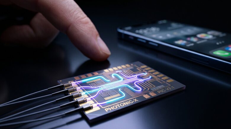
Photonic chips replace electrical signals with laser-generated light pulses to carry and process information. Instead of electrons moving through copper wires, photons travel through microscopic waveguides etched into silicon — structures thinner than a human hair.
The core components of a photonic chip include modulators (which encode data onto light), waveguides (which route it), and photodetectors (which convert light back to an electrical signal for output). This hybrid approach — photons inside the chip, electrons at the edges — is called silicon photonics, and it lets manufacturers use existing semiconductor fabrication lines to produce photonic chips at scale.
Why Light Is Better Than Electricity for Data
Electrons moving through metal generate heat and resistance. Photons in a waveguide do neither. This physical difference means photonic interconnects can carry vastly more data per second according to Intel’s silicon photonics research, without the signal degradation that limits copper at high frequencies. Bandwidth scales with the number of light wavelengths (channels) rather than wire thickness — a principle called wavelength-division multiplexing (WDM).
Key Takeaway: Photonic chips encode data as light pulses through silicon waveguides, achieving transfer rates above 1 terabit per second — a speed impossible for copper-based interconnects without severe heat penalties, making them critical for next-generation AI hardware.
How Do Photonic Chips Compare to Traditional Electronic Chips?
Electronic chips and photonic chips each have distinct strengths. Electronic chips excel at complex logic operations and are supported by decades of tooling. Photonic chips dominate in data movement, signal bandwidth, and energy efficiency for communication-heavy tasks like AI inference and data center interconnects.
The comparison matters most in AI and machine learning, where moving data between processor cores is often the bottleneck — not the computation itself. Photonic chips solve exactly that problem. Lightmatter, a photonic AI startup, reports its Passage interconnect reduces chip-to-chip communication energy by up to 100x compared to electrical alternatives according to the company’s published technical data.
| Feature | Electronic Chip | Photonic Chip |
|---|---|---|
| Data Transfer Speed | Up to ~112 Gbps per lane | 1+ Tbps per waveguide bundle |
| Energy per Bit | ~10–20 picojoules | ~1–2 picojoules |
| Heat Generation | High (resistance-based) | Low (photons generate no heat) |
| Latency | Nanoseconds (electrical) | Picoseconds (optical) |
| Manufacturing Maturity | Fully mature (TSMC, Intel) | Early commercial (Intel, IBM) |
| Best Use Case | General compute, logic | AI interconnects, data centers |
Key Takeaway: Photonic chips consume roughly 1–2 picojoules per bit versus 10–20 for electronic alternatives, a difference Lightmatter’s engineers say translates to 100x lower interconnect energy — critical for data centers where power costs dominate operating budgets.
Who Is Building Photonic Chips Right Now?
The photonic chip industry is no longer a research curiosity — it is an active commercial race. Intel, IBM, Lightmatter, Ayar Labs, and Ranovus are among the leading companies shipping or demonstrating silicon photonic products as of mid-2025.
Intel has shipped silicon photonic transceivers for data centers since 2016 and now integrates photonic interconnects into its Gaudi AI accelerator platform. IBM has published photonic integration roadmaps alongside its quantum computing work. Ayar Labs focuses on optical I/O chiplets that plug directly into existing processor sockets, requiring no chip redesign from the buyer. The U.S. Department of Defense’s DARPA has funded photonic chip research through its PIPES (Photonics in the Package for Extreme Scalability) program, signaling national-security interest in the technology.
The Market Size Signal
The global silicon photonics market was valued at $1.96 billion in 2023 and is projected to reach $9.5 billion by 2030, according to Grand View Research’s 2024 market analysis. That trajectory reflects genuine enterprise demand, not speculative hype.
“Photonics is not a replacement for electronics — it is the missing layer that makes extreme-scale computing physically possible. The chips that win the AI era will be the ones that move data at the speed of light.”
Key Takeaway: The silicon photonics market is on track to grow from $1.96 billion to $9.5 billion by 2030, driven by companies like Intel, Ayar Labs, and Lightmatter — and backed by DARPA’s federal funding for defense-grade photonic integration.
When Will Photonic Chips Reach Consumer Devices?
Consumer-facing photonic chips are roughly 5–10 years away from mainstream adoption, but intermediate benefits will arrive sooner through the cloud. When photonic chips accelerate data center AI servers, every device that connects to those servers — your phone, laptop, or wearable — benefits indirectly from faster, cheaper AI responses.
Direct integration into consumer hardware faces real hurdles. Coupling laser light efficiently into and out of tiny silicon waveguides at low cost remains an engineering challenge. Temperature sensitivity also affects photonic components more than electronic ones. However, breakthroughs in edge computing architectures — where processing moves closer to the user — may bring photonic interconnects into routers, 5G base stations, and local AI processing units within the next decade. If you are curious how edge infrastructure fits into this picture, our explainer on what edge computing is and how it works provides useful grounding.
Near-Term Consumer Impact
The most immediate consumer benefit is latency. AI assistants, cloud gaming, and real-time translation all depend on fast server responses. Photonic data center interconnects reduce round-trip data times, which means snappier app performance — even before photonic chips ever enter your phone. This connects directly to wireless technology improvements; see our breakdown of 5G vs. Wi-Fi 7 for the full picture of network-layer speed gains running parallel to photonic chip development.
Key Takeaway: Mass-market photonic chips in consumer devices are likely 5–10 years away, but cloud-based photonic acceleration already improves app latency today — a dynamic similar to how wearable health devices leveraged cloud AI long before on-device AI chips matured.
Why Do Photonic Chips Matter for the AI-Powered Future?
Photonic chips explained in the context of AI: they solve the data movement problem that is throttling modern AI hardware. Large language models like GPT-4 require moving trillions of parameters between memory and processor cores billions of times per second. Electrical interconnects generate so much heat doing this that cooling consumes a significant fraction of total data center energy.
Photonic interconnects eliminate most of that thermal overhead. Microsoft, Google, and Amazon Web Services have all publicly explored optical interconnect strategies for their next-generation AI server clusters. This is also relevant to the broader discussion of transformative computing paradigms — our article on how quantum computing will change everyday technology explores a complementary track, where quantum and photonic approaches may eventually converge.
Photonic chips explained at the system level also means rethinking chip packaging. Rather than one monolithic processor, future AI systems will use dozens of specialized chiplets connected by optical links — a modular architecture that photonic I/O enables. Ayar Labs calls this concept optical I/O, and it is already being tested in DARPA-funded server prototypes. The performance gains from this architecture are consistent with the storage speed gains consumers already see when comparing traditional hardware, much like the leap documented in our SSD vs. HDD comparison.
Key Takeaway: AI data centers consume enormous energy moving data electrically; photonic interconnects cut that cost by up to 90%, enabling larger AI models at lower operational cost — a shift tracked by industry researchers at Grand View Research as a primary growth driver through 2030.
Frequently Asked Questions
What is a photonic chip in simple terms?
A photonic chip uses light instead of electricity to process and transmit data. Photons travel through microscopic channels etched into silicon, carrying information far faster and with far less energy than electrons moving through copper wires.
Are photonic chips faster than regular computer chips?
For data transfer tasks, yes — photonic interconnects can move data at over 1 terabit per second, roughly 100 times faster than high-end electrical interconnects. For raw computational logic, traditional electronic chips are still more mature and versatile.
What companies are making photonic chips right now?
Intel, IBM, Lightmatter, Ayar Labs, and Ranovus are the leading players as of July 2025. Intel has been shipping photonic transceivers for data centers since 2016. Lightmatter’s Passage chip is aimed directly at AI accelerator interconnects.
Will photonic chips replace silicon chips entirely?
No — not in the foreseeable future. Photonic chips are most effective at data movement and communication, not traditional logic operations. The most likely outcome is hybrid systems where photonic interconnects link clusters of electronic processors, combining the strengths of both.
How does a photonic chip affect my devices today?
Directly, photonic chips are not yet in consumer smartphones or laptops. Indirectly, as data centers adopt photonic interconnects, cloud-dependent services — AI assistants, streaming, cloud gaming — become faster and cheaper for end users.
What is silicon photonics and how does it differ from photonic chips?
Silicon photonics is the specific manufacturing approach that builds photonic components on silicon wafers using standard semiconductor fabrication. All silicon photonic devices are photonic chips, but the term emphasizes compatibility with existing chip factories — which is why Intel and IBM favor this route to commercialization.
Sources
- Nature Photonics — Silicon Photonics Data Transfer Research
- Intel — Silicon Photonics Technology Overview
- Lightmatter — Passage Optical Interconnect Technology
- DARPA — PIPES (Photonics in the Package for Extreme Scalability) Program
- Grand View Research — Silicon Photonics Market Size & Forecast 2024–2030
- IBM Research — Silicon Photonics Integration Roadmap
- Ayar Labs — Optical I/O Chiplet Technology