Fact-checked by the VisualEnews editorial team
Quick Answer
Photonic computing chips use light instead of electrons to process data, offering speeds up to 1,000 times faster than conventional silicon processors while consuming 10–100 times less energy. As of July 2025, companies like Intel, IBM, and Lightmatter are actively commercializing photonic interconnects, with the global photonics market projected to reach $1.2 trillion by 2030.
Photonic computing chips transmit and process information using photons — particles of light — rather than electrical electrons, enabling data to travel at the speed of light through silicon waveguides and optical components. According to Nature Photonics research on integrated photonic processors, prototype photonic chips have already demonstrated data throughput exceeding 100 terabits per second on a single chip, a benchmark no electronic chip has matched.
This matters now because Moore’s Law — the doubling of transistor density every two years — is physically stalling, and AI workloads are demanding exponentially more compute power than silicon can efficiently deliver.
How Do Photonic Computing Chips Actually Work?
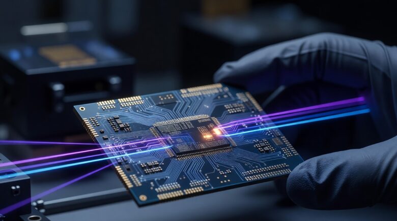
Photonic computing chips encode data as pulses of light, routing signals through microscopic waveguides etched into silicon or indium phosphide substrates rather than copper wires. The fundamental advantage is that photons carry no charge, so they generate almost no heat and experience no electromagnetic interference during transit.
The core components of a photonic chip include laser sources, optical modulators, waveguides, and photodetectors. Modulators switch light signals on and off to encode binary data, while waveguides replace metal interconnects. Companies like Lightmatter and Ayar Labs have pioneered photonic interconnects — optical links that connect processor chiplets — reducing latency between compute units by eliminating copper bottlenecks.
Silicon Photonics vs. III-V Materials
Most commercial photonic chips today use silicon photonics, which leverages existing CMOS semiconductor fabrication lines at foundries like TSMC and GlobalFoundries. However, silicon is a poor light emitter, so researchers at MIT and Stanford University are exploring III-V compound semiconductors such as indium phosphide, which emit light natively and can integrate lasers directly on-chip. According to research published in Applied Materials Today, III-V photonic platforms achieve 40% higher optical efficiency than pure silicon alternatives.
Key Takeaway: Photonic computing chips route data as light through waveguides, generating far less heat than copper-based electronics. Silicon photonics uses existing chip fab infrastructure, but III-V materials deliver up to 40% better optical efficiency for next-generation designs.
Why Are Silicon Chips Hitting a Wall?
Silicon transistors are approaching atomic-scale limits, with leading-edge nodes now at 2 nanometers — roughly the width of 10 silicon atoms. At this scale, quantum tunneling causes electrons to leak across transistor gates, increasing error rates and power draw simultaneously.
The energy cost of moving data has become the dominant constraint in modern computing. Intel estimates that data movement consumes up to 60% of total chip power in large AI accelerators. Copper interconnects inside server racks dissipate enormous heat, requiring expensive cooling infrastructure in data centers. The global data center industry already consumes approximately 200–250 TWh of electricity annually, according to the International Energy Agency’s data center energy report.
Photonic interconnects directly attack this problem. By replacing copper wires with optical fibers or integrated waveguides, energy per bit transferred drops by orders of magnitude. This architectural shift is why NVIDIA, Google DeepMind, and hyperscale cloud providers are funding photonic research aggressively in 2025. It’s a similar paradigm shift to the one explored in our overview of how quantum computing will change everyday technology — both represent post-silicon compute trajectories.
Key Takeaway: Silicon transistors have reached 2nm physical limits, and data movement now accounts for up to 60% of chip power in AI hardware, per IEA energy data — making photonic alternatives an engineering necessity, not just a research curiosity.
| Technology | Data Speed | Energy per Bit | Heat Generation | Commercial Status (2025) |
|---|---|---|---|---|
| Silicon CMOS (2nm) | ~5 Tbps/chip | ~1–10 pJ/bit | High (100–300W TDP) | Mass production |
| Photonic Interconnects | 100+ Tbps/chip | ~0.01–0.1 pJ/bit | Very low | Early commercial (Ayar Labs, Lightmatter) |
| Full Photonic Processors | 1,000+ Tbps (lab) | <0.01 pJ/bit | Near-zero in-chip | Research / pilot stage |
| III-V Photonic Chips | 200+ Tbps | ~0.05 pJ/bit | Low | Pre-commercial (MIT, startups) |
Who Is Building Photonic Computing Chips Right Now?
The photonic computing landscape in 2025 includes both established semiconductor giants and well-funded startups making rapid progress toward commercial deployment.
Lightmatter, a Boston-based startup, launched its Passage photonic interconnect fabric in 2023 and secured a $154 million Series C funding round. Its chips are already being evaluated by cloud providers for AI inference workloads. Ayar Labs has partnered with Intel to integrate optical I/O directly into processor packages, cutting inter-chip bandwidth energy by up to 10x, according to Ayar Labs’ published technical specifications.
On the research side, IBM Research has demonstrated programmable photonic circuits capable of executing matrix multiplications — the core operation in neural network inference — entirely in the optical domain. Microsoft is exploring photonics as a complement to its quantum computing roadmap. Meanwhile, Graphcore and Cerebras Systems are monitoring photonic developments closely as they optimize AI-specific silicon architectures.
“Photonic chips will not replace digital logic overnight, but optical interconnects are the single most important near-term improvement we can make to AI compute infrastructure. The energy savings alone justify the engineering investment at scale.”
Government bodies are accelerating the race. The U.S. Department of Defense DARPA allocated funding through its PIPES (Photonics in the Package for Extreme Scalability) program to advance co-packaged photonics. The European Union’s Horizon Europe program has committed over €1 billion to photonic and quantum hardware research through 2027. This is comparable to the infrastructure investment wave driving the 5G vs. Wi-Fi 7 wireless competition at the network layer.
Key Takeaway: Lightmatter raised $154 million and Ayar Labs has delivered 10x energy reductions in chip-to-chip links, per Ayar Labs’ technical data — signaling that photonic computing chips have moved from lab demos to funded, near-commercial products.
What Are the Biggest Challenges Photonic Chips Still Face?
Despite strong momentum, photonic computing chips face three major unsolved engineering challenges: efficient on-chip light generation, precise optical signal control at scale, and integration with existing digital electronics.
Silicon cannot generate laser light efficiently on its own. Every photonic chip currently requires an external or bonded laser source, adding cost and complexity. Researchers at UC Santa Barbara and startups like QuTech are developing heterogeneous integration techniques — bonding III-V laser dies directly onto silicon wafers — but yields remain low at commercial scales. IEEE Spectrum’s analysis of photonic integrated circuits estimates that heterogeneous bonding defect rates must fall below 0.1 per cm² before volume manufacturing is viable.
Thermal sensitivity is another hurdle. Optical waveguides shift their resonant wavelength with temperature changes as small as 1°C, requiring active thermal stabilization circuits that partially offset the energy savings photonics provide. This is an ongoing area of materials research at NIST (National Institute of Standards and Technology).
The integration challenge is perhaps the most immediate. Photonic chips must still interface with conventional digital processors for control logic. Hybrid electro-photonic architectures — where light handles data movement and silicon handles computation — are the practical near-term path. This parallels the hybrid architecture approach seen in modern storage solutions that blend SSD and HDD technologies for cost-performance balance. Understanding edge computing architectures also helps contextualize where photonic processing fits in distributed systems.
Key Takeaway: Photonic chips require bonded laser sources and active thermal control, with IEEE estimating defect rates must drop below 0.1 per cm² for viable mass production — the field’s most pressing manufacturing barrier as of 2025.
When Will Photonic Computing Chips Replace Silicon?
A full replacement of silicon is unlikely before 2035 at the earliest — but photonic interconnects will enter mainstream AI data centers within the next 3–5 years. The transition will be staged, not sudden.
Phase one, already underway, involves photonic interconnects replacing copper links between chips and between server racks. Phase two, projected for 2027–2030, involves co-packaged optics becoming standard in AI accelerator modules from companies like NVIDIA and AMD. Phase three — fully optical computing with in-chip photonic logic — remains a decade away but is directionally inevitable given the physics of scaling. The U.S. CHIPS and Science Act explicitly funds photonic and advanced packaging research as a national competitiveness priority.
The broader technology curve mirrors transitions we have seen before: just as digital cameras did not eliminate optics but transformed how optics integrates with electronics, photonic computing chips will not erase silicon but will redefine what silicon does. This shift will reshape sectors far beyond data centers — from wearable health technology requiring ultra-low-power sensing chips to next-generation wireless infrastructure.
Key Takeaway: Photonic interconnects are entering AI data centers within 3–5 years, with full photonic processor adoption likely post-2035. The U.S. CHIPS Act is actively funding this transition as a $52 billion national semiconductor strategy.
Frequently Asked Questions
What is a photonic computing chip in simple terms?
A photonic computing chip uses light instead of electricity to move and process data. Photons travel faster than electrons and generate almost no heat, making these chips far more efficient for data-heavy tasks like AI inference and high-speed communications.
Are photonic computing chips available to buy today?
Photonic interconnect products from companies like Ayar Labs and Lightmatter are in commercial evaluation with hyperscale customers as of mid-2025. Full photonic processors that replace all silicon logic are not yet commercially available — they remain in research and pilot stages at institutions like MIT and IBM Research.
How much faster are photonic chips than silicon chips?
In laboratory demonstrations, photonic chips have achieved data throughput exceeding 100 terabits per second, compared to roughly 5 Tbps for leading silicon chips. For specific workloads like matrix multiplication in AI, photonic systems can process operations up to 1,000 times faster than electronic equivalents at equivalent power budgets.
Will photonic chips make AI faster and cheaper to run?
Yes — this is the primary commercial driver. AI inference workloads are dominated by matrix operations and memory bandwidth, both of which photonic architectures handle with far less energy than silicon. Reduced cooling costs alone could cut data center operating expenses significantly as photonic co-packaged optics scale.
What companies are leading in photonic chip development?
The leading commercial players in 2025 include Lightmatter, Ayar Labs, and Intel (through its silicon photonics division). On the research frontier, MIT, IBM Research, UC Santa Barbara, and Stanford University are publishing the most influential work. DARPA’s PIPES program is the key U.S. government accelerator funding this ecosystem.
How does photonic computing relate to quantum computing?
Both use quantum physics at their core, but they solve different problems. Photonic computing targets classical high-speed data processing with light. Quantum photonic computing — a distinct field — uses individual photons to encode qubits for quantum computation. Near-term photonic chips are classical devices and do not require the extreme cooling that superconducting quantum computers need.
Sources
- Nature Photonics — Integrated photonic processors and high-throughput computing
- International Energy Agency (IEA) — Data Centres and Data Transmission Networks Report
- IEEE Spectrum — Photonic Integrated Circuits: Manufacturing and Scaling Challenges
- Ayar Labs — Optical I/O Technology Overview and Energy Specifications
- Applied Materials Today — III-V Photonic Platforms and Optical Efficiency Benchmarks
- Semiconductor Industry Association — U.S. CHIPS and Science Act Overview
- DARPA — PIPES: Photonics in the Package for Extreme Scalability Program