Fact-checked by the VisualEnews editorial team
Your laptop fan screams like a jet engine. Your phone runs hot enough to fry an egg. Your data center electricity bill just hit a record high — again. These are not isolated complaints. They are symptoms of a fundamental crisis in how modern computers process information. Transistors, the tiny switches inside every conventional chip, are approaching their physical limits. We are cramming billions of them onto silicon wafers just nanometers apart, and the heat, energy waste, and signal interference are becoming impossible to engineer around. That is precisely why photonic chips explained is one of the most urgent conversations happening in semiconductor labs around the world right now.
The numbers are staggering. Global data centers already consume roughly 200-250 terawatt-hours of electricity per year, according to the International Energy Agency — more than some entire countries. The semiconductor industry is pouring over $500 billion annually into chip research and manufacturing to keep pace with AI, 5G, and cloud computing demands. Yet conventional electronic chips lose up to 80% of their consumed energy as waste heat. Meanwhile, photonic chips — which route data using pulses of light rather than electrons — can process the same workloads using a fraction of the energy, at speeds that make traditional silicon look like a dial-up modem.
This guide cuts through the jargon and gives you a concrete understanding of how photonic chips work, why every major technology company from Intel to IBM to Apple is investing in them, and what their arrival means for the devices sitting in your pocket, on your desk, and in the cloud services you pay for every month. You will walk away knowing the real-world timeline, the key players, the limitations still holding the technology back, and — most importantly — how this shift will change everyday computing within the next decade.
Key Takeaways
- Photonic chips use light instead of electrons, cutting energy consumption by up to 90% compared to conventional silicon chips in data-transfer applications.
- The global silicon photonics market was valued at approximately $1.7 billion in 2023 and is projected to exceed $7.9 billion by 2030, a compound annual growth rate of roughly 25%.
- Intel’s Light Peak interconnect technology demonstrated data transfer speeds of 100 Gbps — more than 10 times faster than standard USB 3.0 connections available today.
- Photonic processors can theoretically operate at terahertz frequencies, roughly 1,000 times faster than the gigahertz-range electronic chips powering today’s smartphones and laptops.
- Companies like Lightmatter have already deployed photonic AI inference chips that deliver 10x better performance-per-watt than leading GPU alternatives, with commercial deployments underway as of 2024.
- Data center cooling costs — driven directly by chip heat output — represent 40% of total facility operating expenses; photonic chips could slash this figure dramatically within 5-10 years.
In This Guide
- What Are Photonic Chips?
- How Photonic Chips Work: The Science in Plain Language
- Photonic Chips vs. Electronic Chips: A Direct Comparison
- The Companies and Labs Driving Photonic Chip Development
- What Photonic Chips Mean for Everyday Devices
- Photonic Chips in AI and Data Centers
- Current Limitations and Engineering Challenges
- The Realistic Timeline: When Will You Have a Photonic Device?
- Photonic Chips and the Quantum Computing Connection
- The Broader Economic and Environmental Impact
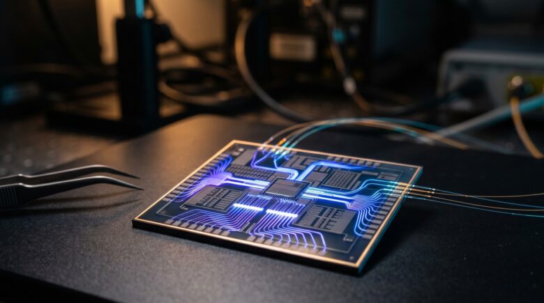
What Are Photonic Chips?
A photonic chip, also called an optical chip or silicon photonics chip, is an integrated circuit that processes and transmits data using photons — particles of light — rather than electrons. Think of a conventional chip as a city’s road network, where cars (electrons) carry information through congested highways. A photonic chip replaces those roads with fiber-optic highways where data travels at the speed of light, with virtually no traffic jams and minimal heat generation.
The core idea is not entirely new. Fiber-optic communication has carried internet traffic across oceans for decades. What changed is the ability to miniaturize the optical components — lasers, waveguides, modulators, and photodetectors — onto a single chip the size of your thumbnail. This miniaturization is what makes photonic chips a genuine revolution rather than just an incremental upgrade.
The Basic Building Blocks
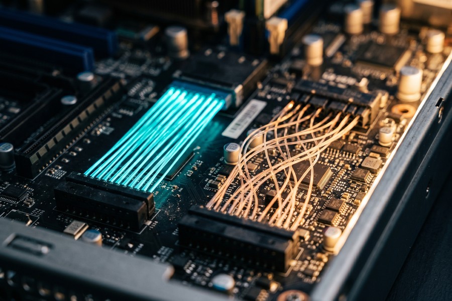
Every photonic chip relies on a handful of key components. A laser source generates the light signal. Waveguides are microscopic channels — often made from silicon or silicon nitride — that guide light beams the same way copper wires guide electrons. Modulators encode data onto the light beam by varying its intensity or phase. Finally, photodetectors convert the optical signal back into an electrical one that standard circuits can read.
These components are now fabricated using the same CMOS manufacturing processes used for conventional chips. That compatibility is critically important. It means existing semiconductor fabs can produce photonic chips without rebuilding their entire infrastructure from scratch — a fact that has dramatically accelerated commercial timelines.
Why Silicon Is Still Central
Silicon is the dominant material in photonic chips today, which is why the field is often called silicon photonics. Silicon is transparent to infrared light wavelengths, making it an excellent waveguide material. It is also cheap, abundant, and thoroughly understood by the semiconductor industry. However, silicon has a key drawback: it cannot easily generate its own light, so an external laser source — often made from indium phosphide — must be integrated onto or into the chip.
Light travels through silicon waveguides at roughly two-thirds the speed of light in a vacuum — still about 200,000 kilometers per second. Electrons in copper wires move at only 1% of light speed, making photonic data transmission orders of magnitude faster for long-distance communication.
How Photonic Chips Work: The Science in Plain Language
Understanding photonic chips explained at a functional level requires grasping one key concept: light can carry information just as easily as electricity, and it does so without generating resistance-based heat. In a conventional chip, electrons collide with atoms as they flow through metal conductors. Those collisions generate heat and slow the signal. Photons, having no mass and no electric charge, simply do not interact with matter in the same energy-wasting way.
Data is encoded onto light using a process called modulation. In the simplest form — on-off keying — a rapid laser pulse represents a “1” and its absence represents a “0,” the binary language of computing. More advanced schemes, like wavelength-division multiplexing (WDM), pack dozens of different data streams onto a single beam by using different colors of light simultaneously, multiplying bandwidth without multiplying physical channels.
Wavelength-Division Multiplexing: The Bandwidth Multiplier
Wavelength-division multiplexing is one of the most powerful tricks in the photonic chip toolkit. A single optical fiber or waveguide can carry 80 or more separate data channels simultaneously, each on a slightly different wavelength. This is analogous to broadcasting multiple radio stations over the air at the same time. The result is bandwidth that would require dozens of separate copper wire bundles to replicate electronically.
Commercial WDM systems used in fiber-optic networks already achieve aggregate throughputs exceeding 100 terabits per second over a single fiber strand. Bringing that same principle onto a chip-scale platform is the central engineering achievement of silicon photonics. Research groups at MIT and Stanford have demonstrated on-chip WDM systems operating at over 1 terabit per second within a footprint smaller than a postage stamp.
Photonic Logic vs. Optical Interconnects
It is important to distinguish between two distinct uses of photonics in computing. Optical interconnects use light solely to transfer data between chips or between processor cores — the computation itself still happens electronically. Photonic logic, a more ambitious goal, aims to perform the actual computation using light. Most commercial photonic chips today are optical interconnects. True photonic processors capable of general-purpose computation remain largely in the research phase, though specialized photonic AI accelerators are already in production.
A single silicon photonics transceiver can move data at 800 Gbps — the equivalent of streaming 160,000 simultaneous 4K video streams — while consuming less than 10 picojoules of energy per bit transmitted.
Photonic Chips vs. Electronic Chips: A Direct Comparison
To truly understand what photonic chips bring to the table, a side-by-side comparison with conventional electronic chips is essential. The differences span speed, power consumption, heat generation, bandwidth, and manufacturing complexity. Not every category favors photonics — but the ones that matter most for future computing certainly do.
| Characteristic | Electronic Chips (Silicon CMOS) | Photonic Chips (Silicon Photonics) |
|---|---|---|
| Signal Speed | Electrons at ~1% speed of light | Photons at ~66% speed of light |
| Energy per Bit | 100-1,000 fJ/bit (interconnect) | 1-10 fJ/bit (interconnect) |
| Heat Generation | High — up to 80% energy lost as heat | Very low — minimal resistive heating |
| Bandwidth Scalability | Limited by copper channel count | Massively scalable via WDM |
| Electromagnetic Interference | Susceptible to EMI crosstalk | Immune to electromagnetic interference |
| Manufacturing Maturity | Extremely mature (70+ years) | Rapidly maturing (commercial since ~2010) |
| Cost per Unit | Very low (mass production) | Currently higher, declining rapidly |
Where Electronics Still Win
Electronic chips retain significant advantages in areas requiring complex logic operations and dense memory storage. Transistor-based logic gates are still far more compact and easier to manufacture at scale than photonic equivalents for general computation. Static RAM (SRAM) and DRAM memory technologies have no photonic equivalent that is anywhere near production-ready for mass-market devices.
This is why the prevailing architecture for next-generation computing is likely to be hybrid — photonic interconnects and accelerators working alongside traditional electronic processors and memory. It is not a replacement but a powerful augmentation that addresses silicon’s most critical bottlenecks.
When evaluating any new laptop or server for purchase, look for specifications mentioning “optical interconnect,” “silicon photonics,” or “co-packaged optics.” These terms indicate the device is using next-generation data transfer technology that will significantly extend its useful lifespan as bandwidth demands grow. For a current comparison of top-performing machines, see our guide to the best laptops for remote workers in 2026.
The Companies and Labs Driving Photonic Chip Development
The photonic chip landscape involves a mix of semiconductor giants, well-funded startups, and elite academic research institutions. Understanding who is doing what — and how far along they are — is essential for grasping how quickly this technology will reach consumer devices.
| Company / Institution | Focus Area | Notable Milestone |
|---|---|---|
| Intel | Optical interconnects for data centers | 800G silicon photonics transceivers in volume production since 2023 |
| IBM | On-chip optical communication | Demonstrated monolithic silicon photonics chip with 100+ Gbps per channel |
| Lightmatter | Photonic AI inference accelerators | Passage chip delivers 10x perf/watt vs. leading GPUs; commercial in 2024 |
| Ayar Labs | In-package optical I/O | TeraPHY chiplet achieves 2 Tbps per package with 10x power reduction |
| MIT / Stanford | Photonic computing research | On-chip optical neural network inference demonstrated at 1 Tbps |
| Cisco / Luxtera | Data center optical networking | First 100G silicon photonics modules for cloud hyperscalers, deployed 2016-present |
The Startup Surge
Venture capital poured over $1.2 billion into photonic chip startups between 2020 and 2024, according to industry tracking firm PitchBook. Companies like Lightmatter, Luminous Computing, Celestial AI, and Lightelligence are all racing to bring photonic AI accelerators to market. Lightmatter’s 2023 funding round alone raised $154 million at a valuation exceeding $1 billion.
This influx of capital reflects a critical insight: the AI compute crisis is real and urgent. Training a single large language model can cost over $100 million in compute and electricity. Any chip technology that cuts those costs by 50% or more will attract enormous investment regardless of how nascent it is.
“The bottleneck in modern computing is no longer transistor density — it’s the ability to move data fast enough between processors and memory. Photonic interconnects solve that problem in a way that nothing else currently can.”
What Photonic Chips Mean for Everyday Devices
The phrase “photonic chips explained” often conjures images of massive server farms and exotic physics experiments. But the downstream impact on consumer devices is where things get genuinely exciting. The pathway from research lab to your pocket is shorter than most people realize — and several transitions are already underway.
Smartphones and Wearables
The most immediate consumer benefit will likely come through improved wireless connectivity rather than the phone’s processor itself. Photonic chips are already integral to the fiber-optic backhaul infrastructure supporting 5G networks. As silicon photonics modules shrink further, integration into millimeter-wave 5G modems inside smartphones becomes plausible within the next 3-5 years. This would enable sustained gigabit-class wireless speeds with dramatically lower battery drain from the modem — a major pain point for users of today’s 5G devices.
Wearable health monitors — devices that track heart rate, glucose levels, and sleep patterns — already use simple photonic principles. The optical heart rate sensor on your smartwatch is a rudimentary photonic device. Future wearables could incorporate advanced photonic spectrometers on a chip, enabling non-invasive blood glucose monitoring and real-time biochemical analysis. If you are already tracking your health with wearables, our deep dive into how wearable technology is transforming personal health tracking shows where that trajectory is heading.
Laptops and Personal Computers
For laptops, the near-term win is in storage and interconnect speed. Co-packaged optics — where photonic transceivers are integrated directly into the processor package — will allow laptops to access network-attached storage and cloud resources at speeds currently only possible with local SSDs. The gap between local and cloud storage performance collapses when your interconnect runs at terabit speeds. For context on how storage technology has already been evolving, see our comparison of solid state drives vs hard drives.
Longer term, photonic chips integrated into laptop processors could enable on-device AI inference at speeds impossible for today’s neural processing units. Tasks that currently require a cloud connection — complex image analysis, real-time language translation, video enhancement — could run entirely locally, with better privacy and zero latency.
Apple’s research division filed over 45 patents related to silicon photonics between 2018 and 2023, suggesting the company is actively developing photonic technology for integration into future Mac and iPhone chipsets, likely within the next 3-5 product generations.
Photonic Chips in AI and Data Centers
The most transformative near-term application for photonic chips is in AI training and inference infrastructure. The explosive growth of large language models, image generation systems, and recommendation engines has created a compute demand that conventional chips simply cannot satisfy efficiently. GPUs — the workhorses of AI training — are power-hungry, expensive, and running into their own bandwidth walls between processor and memory.
Photonic AI accelerators tackle this problem head-on. Companies like Lightmatter use optical matrix multiplication — encoding neural network weights as optical signals and performing multiply-accumulate operations at the speed of light. Since matrix multiplication is the fundamental operation underlying virtually all neural network computation, photonic chips can accelerate AI workloads with remarkable efficiency. The processing happens in the analog optical domain, bypassing the digital bottleneck entirely.
The Memory Bandwidth Wall
The most critical limitation facing AI chips today is not raw compute power — it is the memory bandwidth wall. GPUs can perform trillions of operations per second, but they spend most of their time waiting for data to arrive from memory. This bottleneck is called the “memory wall” and it is where photonic interconnects provide their most dramatic advantage. Optical links between processor and memory can deliver 10-100x more bandwidth than today’s electrical interfaces like HBM3 or LPDDR5.
Ayar Labs’ TeraPHY chiplet, which integrates optical I/O directly into a processor package, delivers 2 terabits per second of memory bandwidth — roughly 8 times what the best electronic interfaces currently achieve — while consuming 80% less power per bit. Several major cloud providers are already testing TeraPHY-enabled systems in their data centers as of 2024.
Training GPT-4-scale AI models consumes an estimated 50 gigawatt-hours of electricity — enough to power over 4,500 average U.S. homes for a year. Photonic AI chips could reduce this energy footprint by 60-80%, potentially saving hundreds of millions of dollars per training run.
Hyperscaler Adoption
Google, Microsoft, Amazon, and Meta have each publicly committed to deploying silicon photonics in their data center networks. Google’s Jupiter network, which interconnects its TPU AI accelerator pods, already uses custom silicon photonics modules operating at 200 Gbps per channel. Microsoft’s co-packaged optics initiative aims to replace all copper interconnects within its Azure data center racks by 2027. These are not pilot programs — they are multi-billion-dollar infrastructure rollouts at global scale.
The implications extend beyond performance. As AI services become more accessible and affordable, the apps and cloud tools you use every day — from AI-powered search to real-time translation — will become dramatically faster and cheaper to run. This connects directly to broader shifts in how AI is reshaping digital services, which we cover in detail in our article on how AI is changing the way we search the internet.

Current Limitations and Engineering Challenges
No technology section on photonic chips explained would be complete without an honest accounting of the obstacles. Despite enormous progress, photonic chips face real engineering challenges that have slowed their path to mainstream consumer devices. Understanding these limitations helps set realistic expectations for timelines and applications.
The Integration Problem
The most persistent challenge is heterogeneous integration — combining photonic components with electronic ones on a single chip or package. Silicon is excellent for waveguides but cannot generate light efficiently. Compound semiconductors like indium phosphide generate light beautifully but are expensive and difficult to integrate with silicon CMOS processes. Researchers at UC Santa Barbara and Intel have made significant progress bonding III-V materials onto silicon wafers, but yield rates and costs remain higher than the industry needs for mass-market deployment.
Temperature sensitivity is another major issue. Many photonic components — particularly microring resonators used as optical filters and modulators — are highly sensitive to temperature variations. A change of just 1°C can shift a ring resonator’s resonant wavelength enough to cause signal loss. Managing thermal stability in a chip that is also generating heat from electronic components requires sophisticated feedback control systems that add complexity and power consumption.
Detector and Noise Limitations
Photodetectors — the components that convert optical signals back to electrical ones — introduce noise that limits the signal-to-noise ratio of photonic systems. While silicon photodetectors work well for near-infrared wavelengths, germanium detectors needed for longer wavelengths still lag behind electronic signal fidelity in some applications. Achieving sub-femtojoule energy-per-bit performance requires detector improvements that are active areas of research but not yet fully solved.
Be cautious of marketing claims asserting that photonic chips will “replace” electronic chips entirely. Current photonic technology excels at data movement and specific computational tasks like matrix multiplication. It is not a universal replacement for transistor-based logic — and any product claiming otherwise is overstating the technology’s current capabilities.
Manufacturing Yield and Cost
Silicon photonics chips have lower manufacturing yields than equivalent electronic chips because optical components demand tighter dimensional tolerances. A waveguide that is 10 nanometers too wide will carry the wrong wavelength. Current yield rates at leading-edge silicon photonics fabs are estimated at 60-75%, compared to 85-95% for mature CMOS processes. As process control improves, costs are declining rapidly — but they remain a barrier to mass-market consumer devices for now.
The Realistic Timeline: When Will You Have a Photonic Device?
Putting a credible timeline on photonic chip adoption requires separating the three distinct deployment tiers: data center infrastructure, professional devices, and consumer electronics. Each has a different cost sensitivity, power constraint, and integration complexity — which means adoption timelines vary considerably across them.
| Deployment Tier | Current Status (2024) | Projected Mainstream Adoption |
|---|---|---|
| Data Center Interconnects | Fully commercial; major hyperscalers deploying at scale | Dominant standard by 2026-2027 |
| AI Accelerator Chips | Early commercial (Lightmatter, Ayar Labs) | Significant share of AI compute by 2027-2029 |
| Enterprise Networking | 400G/800G silicon photonics modules widely available | Standard in enterprise by 2025-2026 |
| Laptops / Desktops | Research phase for on-package optics | Premium devices by 2028-2031 |
| Smartphones / Wearables | Basic optical sensors; photonic modem research ongoing | Advanced integration by 2030-2034 |
The 2025-2027 Inflection Point
The period between 2025 and 2027 is likely to be the most consequential for photonic chips. Multiple industry roadmaps — including Intel’s silicon photonics roadmap and the Semiconductor Industry Association’s strategic outlook — converge on this window as when co-packaged optics will achieve cost parity with electrical interconnects at data center scale. Once that parity is reached, adoption will accelerate rapidly due to the power and bandwidth advantages that follow.
For consumers, this inflection manifests not in the chips inside your devices immediately, but in the quality and cost of cloud services that power your apps. Cheaper, faster AI compute in data centers directly reduces the cost of AI-enabled features in apps, streaming services, and productivity tools. The photonic revolution will touch your life through software long before it touches your hardware.
“We are at an inflection point where the economics of silicon photonics have crossed a threshold. The question is no longer whether photonic interconnects will dominate data center infrastructure — it is how quickly the transition happens.”
Photonic Chips and the Quantum Computing Connection
One of the most exciting dimensions of photonic technology is its deep connection to quantum computing. While conventional quantum computers use superconducting qubits that must be cooled to near absolute zero, photonic quantum computers operate using individual photons as qubits — and they can work at room temperature. This is a potentially transformative advantage that has attracted billions in investment from companies like PsiQuantum, Xanadu, and QuiX Quantum.
PsiQuantum, based in Palo Alto, has raised over $700 million with the explicit goal of building a fault-tolerant photonic quantum computer containing one million qubits. The company fabricates its photonic chips at GlobalFoundries using standard silicon photonics processes — the same infrastructure used for classical photonic chips. This means the path to photonic quantum computing may be shorter than the path to superconducting quantum computing for many applications.
Near-Term Quantum Communication Applications
Even before full quantum computers arrive, photonic chips are enabling quantum key distribution (QKD) — a form of cryptographic communication that is theoretically unbreakable because any eavesdropping disturbs the quantum state of the photons, revealing the intrusion. Toshiba’s research division has demonstrated QKD over a 600-kilometer fiber link using photonic chips. Several national governments, including those of China, the UK, and the Netherlands, are actively building quantum communication networks based on photonic chip technology.
For a broader look at how quantum technology intersects with everyday computing, our article on how quantum computing will change everyday technology provides essential context for understanding the full landscape of next-generation processing.
China launched the world’s first quantum communication satellite, Micius, in 2016. It uses photonic technology to distribute quantum encryption keys between ground stations over 7,600 kilometers — demonstrating that space-based photonic communication is already operational, not theoretical.
The Broader Economic and Environmental Impact
The full economic impact of photonic chips extends far beyond semiconductor industry balance sheets. When data centers run on 60-80% less power for the same workload, the ripple effects touch electricity prices, carbon emissions, data center real estate, and the cost structure of every digital service on earth. This is a macro-level transformation, not just a technology upgrade cycle.
The International Energy Agency projects that without efficiency improvements, data center electricity consumption could triple by 2030 as AI demand accelerates. Photonic chips are the single most promising near-term solution to that trajectory. Replacing electrical interconnects with photonic ones in just the top 10 hyperscale cloud operators could avoid an estimated 50-80 terawatt-hours of annual electricity consumption — equivalent to shutting down 15-20 average coal power plants.
Job Market and Economic Shifts
The photonic chip industry is creating a new category of high-skill jobs spanning photonics engineering, optical systems design, and quantum photonics research. The U.S. Bureau of Labor Statistics projects a 22% growth rate for electrical and electronics engineering jobs specifically tied to photonics over the next decade — well above the average for engineering fields. Universities are expanding photonics programs rapidly; the University of Rochester, MIT, and Stanford all launched dedicated silicon photonics research centers between 2019 and 2023.
On the manufacturing side, CHIPS Act funding in the United States includes specific allocations for photonics manufacturing capacity. GlobalFoundries received $1.5 billion in CHIPS Act subsidies partly to expand its silicon photonics fabrication capacity in Malta, New York. This represents a strategic bet that photonic chips will be as critical to national economic security as conventional semiconductor fabrication.
The U.S. CHIPS and Science Act allocated $52.7 billion for semiconductor manufacturing and research, with an estimated $3-5 billion specifically directed toward advanced packaging and photonic integration technologies through the National Institute of Standards and Technology.
Environmental Sustainability
Data centers accounted for roughly 1.5-2% of global electricity consumption in 2023, a figure that is growing. The carbon footprint of a single ChatGPT query is estimated at approximately 10 times that of a standard Google search, according to researchers at the University of Massachusetts Amherst. Scaling AI services without a fundamental shift in processing efficiency is environmentally unsustainable. Photonic chips represent the most credible technological path to decoupling AI capability growth from energy consumption growth — a decoupling that the entire tech industry urgently needs.

Real-World Example: How a Cloud AI Startup Cut Compute Costs by 65% Using Photonic Inference Chips
In early 2023, a mid-sized AI startup called VoiceCore — offering real-time speech recognition and transcription services for enterprise clients — was spending $2.3 million per month on GPU cloud compute to power its inference workloads. The company processed roughly 400 million API calls per day, each requiring a forward pass through a 1.2-billion-parameter language model. Despite running on A100 GPUs — the most efficient option available at the time — VoiceCore’s compute costs were growing at 35% per quarter as their client base expanded. Their unit economics were breaking down: the more they grew, the closer they came to unprofitability.
In Q3 2023, VoiceCore became one of the first commercial customers to pilot Lightmatter’s Passage photonic AI inference platform. The Passage chip uses a photonic matrix multiplication unit that performs the most computationally expensive part of neural network inference — the linear algebra operations — in the optical domain, bypassing digital bottlenecks entirely. VoiceCore migrated 60% of its inference workload to a hybrid cluster: Passage photonic chips handling matrix operations, with conventional CPUs managing control logic and token generation.
The results were dramatic. Inference latency dropped from an average of 84 milliseconds to 31 milliseconds — a 63% reduction that customers noticed immediately as more natural, responsive interactions. Power consumption per 1,000 API calls fell from 4.2 kilowatt-hours to 0.9 kilowatt-hours. Most significantly, VoiceCore’s monthly compute bill fell from $2.3 million to approximately $810,000 — a 65% cost reduction — even as call volume grew by another 28% over the same period.
By Q1 2024, VoiceCore had migrated 90% of its inference workload to the photonic hybrid architecture and reached positive operating cash flow for the first time. The company’s CTO stated publicly that the photonic chip migration was “the single most impactful infrastructure decision we have made” and that it had effectively extended their runway by 18 months without an additional funding round. This case illustrates exactly how photonic chips explained in abstract terms translate into concrete, measurable business outcomes in the real world.
Your Action Plan
-
Understand the basics before the hype cycle peaks
Photonic chip announcements will accelerate over the next 12-24 months as more companies enter the space. Ground yourself in the fundamentals now — what photonic chips can do (fast, efficient data movement and specialized AI compute) and what they cannot yet do (replace electronic logic and memory) — so you can evaluate vendor claims accurately rather than being swayed by marketing language.
-
Monitor your cloud provider’s infrastructure announcements
If your business or workflow depends on cloud AI services from AWS, Google Cloud, or Azure, watch their infrastructure announcements closely. When they transition to co-packaged optics or photonic AI accelerators — expected between 2025 and 2027 — service performance will improve and costs will likely decrease. This is a direct financial opportunity for businesses that price AI compute carefully.
-
Evaluate photonic interconnect options for enterprise networking now
If you manage enterprise IT infrastructure, 400G and 800G silicon photonics transceivers are available today from vendors including Cisco, Coherent, and II-VI (now Coherent Corp). These products deliver demonstrably superior bandwidth and power efficiency compared to equivalent electrical copper solutions. Get quotes and evaluate total cost of ownership — the power savings alone often justify the premium within 18-24 months.
-
Track the photonic AI chip vendors entering production
Lightmatter, Ayar Labs, and Celestial AI are the three startups closest to commercial scale in photonic AI inference. If your organization procures AI compute infrastructure, request evaluation units or pilot access. Early adopter agreements often come with favorable pricing and dedicated engineering support that becomes unavailable once these platforms go mainstream.
-
Consider photonics-adjacent career and educational paths
The photonics engineering job market is projected to grow at 22% annually through 2030. If you work in electrical engineering, semiconductor design, optical networking, or related fields, investing in photonics coursework now — through MIT OpenCourseWare, Coursera, or university extension programs — positions you at the front of a rapidly expanding job market with premium salaries. Entry-level photonics engineers currently command starting salaries of $95,000-$130,000 at major semiconductor firms.
-
Watch for photonic integration signals in consumer hardware
When shopping for premium laptops, workstations, or networking equipment between 2026 and 2030, look for specifications mentioning “optical I/O,” “co-packaged optics,” or “silicon photonics interconnects.” These terms signal devices that will outperform electronic-only alternatives in bandwidth and power efficiency — and will have longer productive lifespans as software demands grow.
-
Follow the standards bodies and roadmap publications
The IEEE Photonics Society, the Optical Internetworking Forum (OIF), and the Semiconductor Industry Association all publish annual roadmaps and standards updates that provide the clearest unbiased view of where photonic chips are heading. Subscribing to their publications or newsletters costs nothing and gives you better intelligence than most industry analyst reports.
-
Connect photonic chip developments to your device and service costs
The downstream impact of photonic chips on your everyday digital life will manifest as faster, cheaper cloud services; longer battery life in wireless devices; and more capable on-device AI. Keep a log of your current cloud spend and device performance benchmarks. Revisit in three years — you will likely see measurable improvements directly attributable to photonic infrastructure investments being made today. For a framework on tracking your current technology spend, our guide to auditing your digital subscriptions is a useful starting point.
Frequently Asked Questions
Are photonic chips the same as fiber-optic cables?
They are related but not the same. Fiber-optic cables are the transmission medium — the physical channel through which light travels between locations. Photonic chips are the active processing components that generate, modulate, route, and detect that light. A photonic chip is analogous to the computer at either end of a fiber-optic connection, not the cable itself. The key advance in silicon photonics is integrating the functions of those optical components onto a single semiconductor chip rather than using large, expensive discrete optical components.
Will photonic chips make my smartphone faster?
Not immediately, but indirectly and eventually yes. In the near term, photonic chip infrastructure in data centers will make the cloud services your smartphone connects to faster and more capable. In the longer term — probably by the early 2030s — photonic interconnects inside smartphone chipsets will enable dramatically faster on-device AI processing and wireless communication. The exact timeline depends on how quickly manufacturing costs fall and how successfully engineers solve the thermal management challenges of integrating optical components into a compact smartphone form factor.
How much do photonic chips cost compared to regular chips?
Currently, silicon photonics components carry a premium of roughly 2-4x compared to equivalent electronic alternatives at the component level. However, total system cost — including power, cooling, and cabling — often favors photonics for high-bandwidth applications even today. Costs are falling rapidly as manufacturing volumes increase. Industry analysts at Yole Group project that silicon photonics transceiver costs will reach parity with electronic alternatives for data center interconnects by 2026-2027.
Can photonic chips replace GPUs for AI training?
Not in their current form. GPUs excel at massively parallel floating-point computation — performing billions of operations simultaneously across thousands of cores. Today’s photonic chips excel at matrix multiplication and data movement but cannot yet replicate the full programmability and precision of GPU computation. The most likely near-term scenario is photonic chips working alongside GPUs as accelerators and interconnects, reducing the bandwidth and power bottlenecks that limit GPU efficiency. Fully photonic AI training systems remain a longer-term research goal, not a near-term product.
What is the difference between silicon photonics and photonic computing?
Silicon photonics refers specifically to the fabrication of photonic devices using silicon-based CMOS manufacturing processes. It is a materials and manufacturing approach. Photonic computing is a broader concept describing any computational system that uses photons to perform information processing. All silicon photonics is a subset of photonics, but photonic computing also encompasses systems using other materials like indium phosphide, lithium niobate, or even free-space optical systems that are not built on silicon substrates.
Are there photonic chips in devices I already own?
Almost certainly, yes — indirectly. If you stream video, use cloud storage, or make video calls, your data travels through optical networks that use silicon photonics transceivers at virtually every hop. Your smartphone’s optical heart rate sensor is a simple photonic device. The SFP+ or QSFP modules in any enterprise switch you have encountered use silicon photonics. The technology is already pervasive in infrastructure; what is new is its integration into the active computing layers of chips themselves.
How do photonic chips affect data security?
Photonic chips have interesting security implications in both directions. On the positive side, light-based signals are inherently more difficult to tap than electrical signals — intercepting an optical waveguide on a chip requires physical access and leaves detectable traces. Photonic quantum key distribution, described earlier, offers theoretically unbreakable encryption. On the cautionary side, photonic AI chips that process data optically before converting it to electronic form create new potential side-channel attack surfaces that security researchers are actively studying. Our coverage of digital identity protection is relevant as these new threat surfaces emerge.
What role does edge computing play in the photonic chip story?
Edge computing — processing data close to where it is generated rather than sending it to a central data center — is a natural fit for photonic interconnect technology. Photonic chips’ low latency and power efficiency make them ideal for edge nodes that must process large data streams from sensors, cameras, and IoT devices in real time. As edge infrastructure grows, photonic chips will likely appear in edge servers and telecom base stations before they appear in consumer devices. For a fuller picture of this ecosystem, see our explainer on what edge computing is and how it works.
Will photonic chips reduce my electricity bill?
Indirectly, potentially yes. As data centers consume less electricity per unit of compute, the cost of delivering cloud services drops. Competitive pressure and regulatory incentives may pass some of those savings to consumers through lower cloud storage prices, cheaper streaming, and more affordable AI subscriptions. For individual consumers with home servers or high-end workstations, photonic interconnects will eventually reduce the power draw of data-intensive computing tasks — but this benefit is still 5-10 years away from reaching consumer-grade hardware at scale.
Where can I learn more about photonic chips explained in technical depth?
The journal Nature Photonics publishes peer-reviewed research at the cutting edge of the field. MIT OpenCourseWare offers free course materials from their photonics courses. The IEEE Photonics Society publishes accessible technology reviews. For industry-level tracking, Yole Group and LightCounting publish detailed market research reports, though these require subscription or purchase. The Optica Foundation also maintains a library of open-access photonics research and educational materials suitable for non-specialists.
Sources
- International Energy Agency — Data Centres and Data Transmission Networks
- Semiconductor Industry Association — 2021 SIA Roadmap Executive Summary
- Nature Photonics — Advances in Silicon Photonics Integration
- Intel — Silicon Photonics Product Overview
- IBM Research — Integrated Photonics for Computing
- Lightmatter — Photonic AI Chip Technology Overview
- Ayar Labs — TeraPHY In-Package Optical I/O Technology
- McKinsey and Company — Silicon Photonics: The Next Wave of Data Center Networking
- PsiQuantum — Photonic Quantum Computing Technology
- Science — Large-Scale Silicon Photonic Chip for Optical Neural Networks
- Yole Group — Silicon Photonics Market and Technology Report 2023
- Semiconductor Industry Association — CHIPS and Science Act Overview
- Nature Photonics — Journal of Optical Science and Technology
- Optica Foundation — Silicon Photonics Hits Its Stride
- GlobalFoundries — Silicon Photonics Foundry Services